Imaging of electrons moving around at 80,000m per second in semiconductor
Published: October 29, 2014
Summary
Postdoctoral fellow Keiki Fukumoto, together with researcher Ken Onda and Professor Shinya Koshihara, all of the Graduate School of Science and Engineering at the Tokyo Institute of Technology, succeeded in direct observation and video imaging of electron flow at 80,000m per second in a semiconductor. They did so by combining a new laser pulse light source and a photoemission electron microscope (PEEM) to develop an ultra high-speed microscope that enabled visualization of electrons on a 20 nanometer (nm, 1nm is 1/100,000,000m) and 200 femtosecond (fs, 1fs is 1/1,000,000,000,000,000s) scale.
Semiconductors are widely used in PCs, mobile phones and solar batteries, and have become indispensable, but there had been no method to view the movement of the carriers (electrons) that controlled their behavioral functions.
With the advance of the nano-sizing of semiconductor elements, attention is on the development of elements (transistors, solar batteries, LEDs, quantum computers) that use the resulting quantum size effect. Devices able to visually assess that electrical conductivity are expected to have a major impact on future semiconductor element development.
The results of this research were published in the online bulletin version of the American scientific journal "Applied Physics Letters" on March 7.
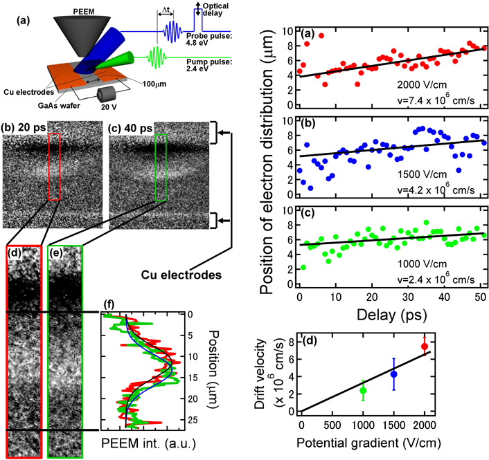
Fig. 1
Time-resolved PEEM video imagery of electron movement. (a): Outline of measurement method. (b)&(c): Photoelectron microscope images after laser irradiation at 20ps and 40ps. (d)&(e): Magnifications of the center areas of (b)&(c). (f): Electron movement can be confirmed from the vertical-direction profiles in (d)&(e).
Fig. 2
(a),(b),(c) are the movement ranges for electrons plotted against time using the electric field gradient between different electrodes (voltage value ÷ electrode interval). The movement speed of the electrons is calculated from the linear fit inclination. (d) is electron movement speed plotted against the electric field gradient.
Reference
Authors: |
Keiki Fukumoto, Yuki Yamada, Ken Onda and Shin-ya Koshihara |
Title of original paper: |
Direct imaging of electron recombination and transport on a semiconductor surface by femtosecond time-resolved photoemission electron microscopy |
Journal: |
Appl. Phys. Lett. 104, 053117 (2014) |
DOI: |
|