Innovative technology to recover performance of CMOS devices damaged by hot carrier injection
Published: March 12, 2015
Tokyo Tech researchers demonstrate for the first time that application of pulsed reverse-voltages produce recovery of the performance of CMOS transistors damaged by the generation of electron-traps in the gate oxide due to hot carrier injection (HCI) of highly energetic electronics from the source-drain region.
The tremendous reduction in the dimensions of transistors has enabled the fabrication of ultra-high density electronic circuits. However, advances in integrating more CMOS devices into smaller areas have led to the degradation of device performance due to the injection of high energy electrons into ultra-thin gate oxide regions of the devices. This degradation of CMOS devices is due to the generation of traps in the gate oxide due to the injection of so-called hot carriers. Currently, the recovery of damage induced by hot carrier injection in CMOS devices is carried out by high temperature thermal annealing of devices; a procedure that requires additional equipment, hence is costly and time consuming. So there is demand for simpler, economical, and rapid on-chip methods to restore the performance of nano-meter scale CMOS devices.
Here, Professor Akira Matsuzawa, Associate Professor Kenichi Okada and colleagues at the Graduate School of Science and Engineering, Tokyo Institute of Technology have developed an innovative "pulsed reverse voltage" method to recover the electrical characteristics of high performance CMOS transistors damaged due to hot carrier injection effects induced by high energy electrons entering and damaging the gate oxide as they traverse between the source and drain of these transistors.
Notably, the researchers demonstrated the practical applications of their method for recovering the performance of CMOS devices by incorporating their technology into CMOS circuits and successfully recovering the output power of millimeter wave band radio devices fabricated devices using a 65 nm pitch CMOS process.
These results were reported at 2015 IEEE International Solid-State Circuits Conference (ISSCC 2015), San Francisco, 22-26 February 2015.
Summary of expriments and findings
- Experiment to recovery the performance of 60-GHz CMOS transceiver damaged by hot carrier injection (HCI).
- Performance recovery technology applied to a millimeter-wave power amplifier as shown in Figure 1.
- The transistor module consists of a core NMOSFET with deep n-well, a tail switching transistor, a MIM transmission line (MIM TL) with a MIM capacitor array attached alongside, and a high-density decoupling capacitor.
- Figure 2 demonstrates the recovery from hot carrier injection for a 60-GHz CMOS transceiver. After the recovery operation is applied, a significant recovery of the output power is observed.
- Figure 3 shows the die micrograph. The transceiver is fabricated in a 65nm CMOS technology. The core areas of the transmitter, receiver, PLL and control logic are 0.79mm2, 1.01mm2, 0.27mm2, and 0.21mm2, respectively.
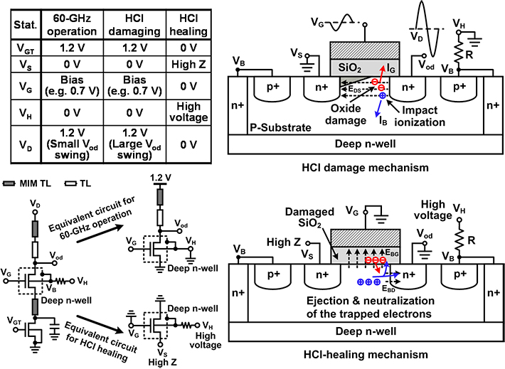
Figure 1: Proposed HCI damage healing technique for PA.
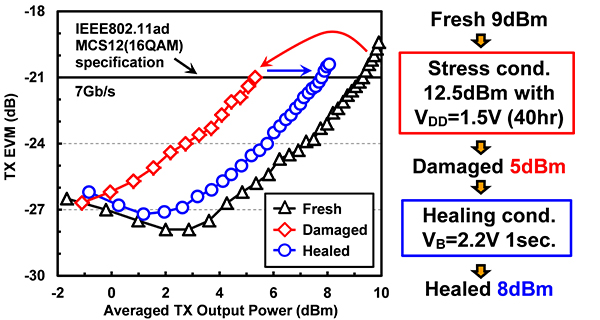
Figure 2: Measured TX EVM and output power of 60GHz Transceiver.
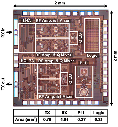
Figure 3: Die micrograph.
Reference
Authors: |
Rui Wu, Seitaro Kawai, Yuuki Seo, Kento Kimura, Shinji Sato, Satoshi Kondo, Tomohiro Ueno, Nurul Fajri, Shoutarou Maki, Noriaki Nagashima, Yasuaki Takeuchi, Tatsuya Yamaguchi, Ahmed Musa, Masaya Miyahara, Kenichi Okada and Akira Matsuzawa |
Title of original paper: |
"An HCI-Healing 60GHz CMOS Transceiver", Session 19 - Advanced Wireless Techniques |
Journal: |
2015 IEEE International Solid-State Circuits Conference (ISSCC 2015) |