Tokyo Tech researchers uncover unusual effects on the electronic structure of TMDs.
The time may be coming when the rapid increases we have witnessed in the last several decades will no longer be possible. Integrated circuits have become smaller and smaller to allow for faster processing, but we are now approaching the size limits for these components.
Although quantum computing and spintronic devices promise further advances, many obstacles remain. Materials and devices capable of handling and preserving the "spin" of electrons are needed to making these technologies directly useful. Transition-metal dichalcogenides (TMDs) are unique layered semiconductors. When these materials are thinned down to monolayers, as similar to graphene (carbon monolayer) from graphite, they have been shown to have a number of interesting and unusual electronic and optical properties, which have been exploited by in many new electronic devices.
However, the biggest challenges toward practical applications are how to prepare high-quality and large-area monolayer functional materials and how to understand the working principle of the devices using them.
Knowing how things work
To understand how a TMD semiconductor behaves inside a device, a multinational collaboration (UK, Japan, Thailand, Germany, and USA) with members from Tokyo Tech (Takao Sasagawa and others) has investigated the effects of sub-monolayer deposition of alkali atoms (Rb) at the surface of the semiconductor tungsten selenide (WSe2). These deposited atoms mimics the electric field effects that a semiconductor would experience inside a transistor, while allowing researchers to directly analyse the electronic structure by a state of the art spectroscopic technique.
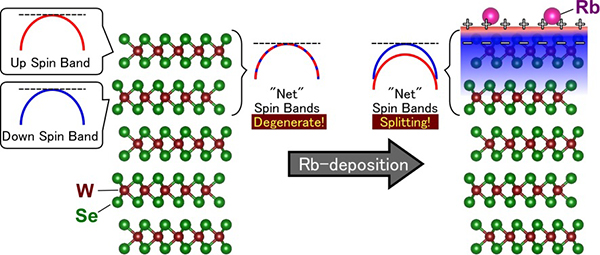
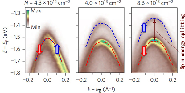
The authors showed that the build-up of charge from the Rb atoms occurred only on the surface monolayer of WSe2, which significantly changed the band structure. This change in the surface electronic states avoids the overlapping of spin-dependent band structures between the topmost layers and the bulk of the material (Figure 1), resulting in the giant and tunable energy splitting of the spin states (Figure 2).
Figure1.
Schematic showing the "chemical gating" effect by the alkali metal (Rb) deposition on the surface of a WSe2 crystal: the formation of a monolayer electron gas with spin band splitting takes place.
Figure2.
Angle-resolved photoemission spectroscopy reveals changes in the energy band structure at the surface of a WSe2 crystal with increasing the carrier density (N) by the alkali metal (Rb) deposition.
This is very good news for device applications in that, without the laborious monolayer fabrications, the spin functionality specific to monolayers can be realized using (high-quality and large-area) bulk crystals by the simple deposition process. Curiously, the induced surface electronic states were found to be unusual: they showed the so-called negative electronic compressibility, behaving something like a counterintuitive "drop" of water level even by "pouring" water.
Knowledge is key
The new insight into the behaviour of these semiconductors in a device-like environment explains many of the interesting properties of WSe2. This breakthrough is an important step in making next generation computing a reality.
Reference
Authors: |
J. M. Riley, W. Meevasana, L. Bawden, M. Asakawa, T. Takayama, T. Eknapakul, T. K. Kim, M. Hoesch, S.-K.Mo, H. Takagi, T. Sasagawa, M. S. Bahramy and P. D. C. King |
Title of original paper: |
Negative electronic compressibility and tunable spin splitting in WSe2 |
Journal: |
Nature Nanotechnology |
DOI : |
|