Special ReportPart 2
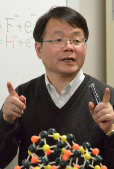
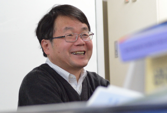
ProfessorHideo Hosono
Frontier Research Center Director
Materials Research Center for Element Strategy
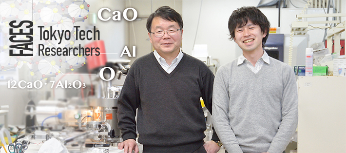
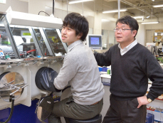
Professor Hideo Hosono is a leading candidate for the Nobel Prize for his research on iron-based superconductors. He has been focusing on transparent oxide materials in his research and made significant achievements. One such material, C12A7 (12CaO·7Al2O3), a constituent of alumina cement, is at the heart of all of his research. Professor Hosono spoke about the allure of transparent materials and their potential as well as about his research achievements.
FACES: Tokyo Tech Researchers, Special Report - Hideo Hosono, Part 1
Electric current passed through a transparent amorphous oxide material!
I heard that you were doing research on transparent oxides before
you began research on superconductivity.
I am still researching them. The clear crystal glasses used for drinking whiskey are sparkly and beautiful, wouldn't you say? I love transparent materials. I've been researching them ever since I was in graduate school, trying to somehow relate them to electrons. In 1993, I moved to Tokyo Tech as an associate professor. That was when my research partner at the time, Professor Hiroshi Kawazoe (currently professor emeritus), had just begun research on new transparent conductive oxides. Until then I had been working on photonic glass at the Nagoya Institute of Technology, but when I came to Tokyo Tech, I was able to continue research on transparent materials.
You then discovered a transparent amorphous oxide semiconductor which
led to the creation of the IGZO semiconductor. Is that correct?

I began research on transparent amorphous oxides around the time that Masahiro Yasukawa, now a professor in the Department of Materials Science and Engineering at Kochi National College of Technology, obtained his experimental results. While searching for a new transparent oxide semiconductor made of crystal, he discovered that an amorphous thin film of silver antimonite (AgSbO3), which he had obtained by chance, had electron mobility that was comparable to that of crystal. Amorphous materials are non-crystalline, that is, the atoms are not regularly aligned. In technical terms, they are materials that display no sharp peaks in x-ray diffraction. At the time, it was commonly believed that unless a material has atoms that are nicely aligned, like crystal silicon (Si), electrons could not move smoothly for electricity to flow. Research on amorphous silicon was being actively conducted, but it was understood that, compared to crystalline silicon, it was much harder for electrons to move. Therefore, no one thought that amorphous oxides, which are insulators in most cases, could make superior semiconductors.
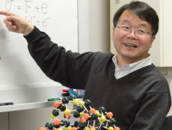
It was reasonable for people to dismiss the potential of amorphous oxide semiconductors and assume that they would be far inferior to crystalline semiconductors even if such materials could be created. But I had a good feeling that this was going to be it. I started thinking about how amorphous oxides could have high electron mobility and immediately came up with a model. This was a model for a materials system that allowed electrons within amorphous oxides to be as mobile as they are in crystal - a system which later led to the creation of the IGZO semiconductor. To explain it simply, until then it was believed that in order for electrons to move smoothly, atoms had to be nicely lined up as they are in crystal. But I noted that it would be sufficient to have well-linked metal ion orbitals (the spaces where electrons can enter and move). It's easy to understand if you think of the orbitals of atoms as metal balls. Imagine a string of metal balls. When the balls are lined up straight, they represent a crystal; when they are in a state of disarray, they are amorphous. However, as with the metal balls, the orbitals of electrons are spatially spread out and spherical in shape, and if one makes contact with its neighbor, the electrons, even when in disarray, are still able to move smoothly. The orbitals of atoms can take various shapes, and these shapes and the spacing of the orbitals are important (see Column 1).
Column 1: Why certain materials are able to conduct electricity well even if they are amorphous (non-crystalline).

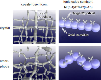
Figure 1. The paths traversed by electrons in covalent and ionic semiconductors
With ionic oxide semiconductors, the spherical s orbitals of the p-block metals overlap nicely in both the crystal and amorphous states. With covalent semiconductors, the orbitals overlap perfectly in the crystal state, but they are hardly able to keep such well overlapping positions in the amorphous state due to the high anisotropy of orbitals and structural randomness.
Atoms each have a set number of electrons that exist in small regions called orbitals. Orbitals have various shapes and spacing, which are determined by the type of atom. When two atoms join together, or couple, their orbitals overlap closely. Electrons move where orbitals overlap, so electricity flows.
For example, in the case of silicon, which is often used as a semiconductor, the orbitals overlap in the crystalline state as shown in the top left image of Figure 1. Silicon orbitals have an orientation, so when silicon is in the amorphous (non-crystalline) state, the overlapping regions become small. As a result, electricity is not able to flow as nearly as well as they can in the crystalline state.
On the other hand, consider ionic materials where coupling occurs in spherical orbitals that are spatially spread out such as the s orbital of p-block cation (see images on the right in Figure 1). In this case, the materials may become amorphous with irregular alignment of atoms, but that would have little effect on the path of the electrons (the overlapping orbitals) as long as the spherical orbitals are spread out widely. As a result, electricity is able to flow seamlessly even in the amorphous state. Professor Hosono noticed this and identified the combinations of atoms that have such orbitals in his paper.
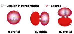
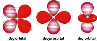
Figure 2. Types and shapes of electron orbitals of atoms
Electrons in atoms each move along specific orbitals.
I understand that this material has already been put to practical use.
You must be referring to IGZO. It's an oxide semiconductor composed of indium, gallium, zinc and oxygen. It has begun to be used in tablet PCs, smart phones, and, recently, large organic EL televisions. In 1996, when we published a paper on amorphous oxides, we specifically mentioned which metal oxides can have high mobility even when they are amorphous. Among them were of course indium, gallium and zinc. IGZO allows a high-density ceramic material to be easily prepared, and by using a common method called sputtering, thin films can be made from this material on a large-sized glass plate. I think that this is one of the primary reasons why IGZO was put into practical use very quickly among a variety of candidate materials I proposed.
The world's reaction must have been amazing when your paper was published.

There was almost no reaction [laughter]. I presented the paper at the International Conference on Amorphous Semiconductors held in August 1995 in Kobe. That was when amorphous silicon was at its zenith, so there were around 800 papers presented, but mine was the only one on amorphous oxides. The reaction to it was all but non-existent. However, when our article appeared in Nature in 2004, we got a great reaction. In the article, we used IGZO as an example to show that thin film transistors (TFTs) made of transparent amorphous oxide have ten times the mobility than those made of amorphous silicon. There was a demand for semiconductors that could be easily made into TFTs with greater mobility. Ten years after the conference in 1995, I gave a presentation on amorphous oxide semiconductors at a plenary session of the same conference held in Lisbon. The General Chair was a researcher from Europe who remembered my presentation in 1995. I prefaced my presentation by saying, "This is a kind of revenge for the lack of reaction to my talk at the conference in 1995." It was an emotional moment for me.
What do you think the future holds for amorphous oxides?
Around the year 2000, flexible transistors and devices fabricated on plastic substrates characterized as "flexible electronics" started being researched extensively. They are based on organic semiconductors, but I believed amorphous oxides would be much superior for flexible electronics applications. In particular, they have much greater mobility than organic semiconductors. They are also much more chemically stable. At present, high-definition technology used in IT devices are rapidly advancing, and materials with high electron mobility will become critical to accommodate this. Needless to say, transparent semiconductors are particularly suitable for application in conventional displays.
I actually would like to see transparent amorphous oxide semiconductors used to make large organic EL displays. Organic EL displays are said to be the next-generation display technology that will replace LCDs, but they still face certain technical obstacles. In addition to the unevenness and instability of the pixels, they cannot compete with LCDs in terms of how large they can get. I think these problems could potentially be solved by using new materials, namely transparent amorphous oxide semiconductors.
Promotion of university-developed technology
I wish Japanese companies would be more aggressive in putting the results of basic research conducted at Japanese universities and research centers to practical use. If they could mention that they're using university-developed technology, that would go a long way toward increasing the motivation of young researchers and students.
The C12A7 electride catalyst would change
the 100-year-old ammonia synthesis process
Is it true that there is a go-to material in your materials research?

C12A7(12CaO・7Al2O3)
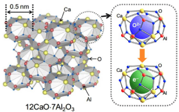
Figure 3
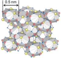
There is a material that has been a staple of my research for about 30 years (see Figure 3). It is a material called C12A7 (12CaO·7Al2O3), which is a constituent of alumina cement, and it's of course transparent (in powder form it's white). It's endlessly fascinating. It's kind of like a toy chest for me. For example, C12A7 was initially an insulator, but I tried to change its electrical properties by replacing oxygen ions accommodating its crystal structure with electrons. When I did that, it first became a transparent semiconductor, then it became a metal (when the temperature is lowered, electrical resistance is decreased), and in 2007, it also became a superconductor.
The wonders hidden in undergraduate laboratory experiments
When I was a newly minted assistant professor at the Nagoya Institute of Technology, I oversaw undergraduate student experiments. A colleague of mine in a neighboring division was overseeing an experiment involving the synthesis of C12A7. When I went there to shoot the breeze, I noticed something interesting. C12A7 is made by mixing, melting and then solidifying calcium carbonate and alumina. From its molten state at a high temperature, it is cooled and solidified. At this temperature, it was supposed to become colorless, but I noticed that it became deep yellow. Then, it was rapidly cooled until it turned into transparent glass, but when it was heated again, an enormous number of bubbles (containing oxygen gas) were generated in the entire sample. I wanted to know why these seemingly strange phenomena occurred in such a commonplace material, and wound up taking up this subject as my own research topic. You may be surprised that there are new discoveries hidden in student experiments, but I think there are many elementary things that we actually don't understand. Since then I have tried various things on this cement material. Nowadays it's become somewhat famous as a multifunctional material, and I think I deserve some credit for that [laughter].
This material has now become a catalyst for ammonia synthesis, right?

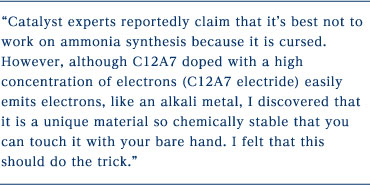
It's well known that ammonia (NH3) is an important component of fertilizers. In recent years, however, its value has risen as a storage material for hydrogen (H2), which is used in fuel cells. Hydrogen is a gas so its volume is large, which makes it difficult to store and transport. But if it can be stored in the form of liquid ammonia and then separated out when necessary, the problem can be solved. Since about 100 years ago, ammonia synthesis has been carried out using the Haber-Bosch process. There have been researchers who took on the challenge of developing a new method of ammonia synthesis, but nobody has succeeded in replacing the Haber-Bosch process. The subject of ammonia synthesis is thus said to be cursed.
Why is the Haber-Bosch process so difficult to replace? The reason is that, in order to synthesize ammonia, it is first necessary to break the strong triple bonds of nitrogen molecules (N≡N) and convert them into two nitrogen atoms. To do that, I theorized that a material that has two contradictory properties would be effective, namely a material that transfers electrons easily, like an alkali metal, but doesn't react with nitrogen. The C12A7 electride is a material that has both of these properties. So, with its surface supported by minute particles of ruthenium to capture N2 - an idea first proposed by the late Professor Emeritus Atsumu Ozaki and Professor Emeritus Ken-ichi Aika of Tokyo Tech - we tested it as a catalyst. As a result, the ammonia synthesis reaction proceeded smoothly (see Column 2).
Column 2:

The manufacture of ammonia is still conducted by the Haber-Bosch process, which was adapted for industrial use a hundred years ago. Since then, small improvements have been made to the process. However, if the elevated pressure and temperature requirements of 200 - 1000 atmospheres and 400 - 600 ℃ are not satisfied, the synthesis reaction will not proceed efficiently. This process thus requires a large amount of energy. Professor Hosono is aiming to develop a catalyst that will enable ammonia synthesis under rather different conditions. The material that is the basis of the catalyst, C12A7 electride (12CaO·7Al2O3 doped with a high concentration of electrons), is a cement material made from lime and alumina. It is composed of numerous cage-like structures. Initially, oxygen ions (O2-) are inside these structures. However, when heated together with titanium metal, the oxygen ions join with the titanium and easily escape, after which electrons (e-) enter. The electrons are easily transferred outside the cages, so they can transfer to the nitrogen molecules (N≡N) and break the strong triple bonds. As a result, with this catalyst, ammonia can be synthesized at 1 atmosphere and 400 ℃. Professor Hosono believes this temperature may be lowered further.
This material consists of cage-like structures and various atoms and electrons can be contained within them. In the case of electrons, however, they are loosely bound when they enter, so they can easily get out. The ammonia synthesis catalyst uses this property. With this catalyst, it should be possible to synthesize ammonia with 10 times the efficiency of the traditional method.
It must have been difficult to develop an ammonia synthesis catalyst that
competes with a 100-year-old method.
Of course, it wasn't easy, and our research is only in the preliminary stages. The Haber-Bosch process is not such an easy process to replace. After all, it is considered a monumental achievement. We want to create a process that can synthesize ammonia under simple conditions - under ordinary pressure and at as low a temperature as possible - and in a place where hydrogen can be obtained on-site. After about ten years and many failed attempts, I was able to make this material into a catalyst. With ammonia synthesis, the key is the transfer of electrons, so the surface where nitrogen and the catalyst meet is important. Therefore, I needed to somehow observe the surface of the C12A7 electride at the atomic level. Some people told me that this was probably impossible since the material has a complicated crystalline structure with no cleavage. But Yoshitake Toda, who at that time was a third-year doctoral student (currently a specially appointed lecturer), really worked hard on it, and in 2010, we were able to observe the surface structure of the material using a scanning tunneling microscope (we were also greatly helped by Professor Hiroyuki Hirayama, an expert in surface science). As a result, I was able to understand why using C12A7 electride as a catalyst hadn't gone well until then. As it turned out, the cages on the surface were broken and the electrons couldn't go into them. Since I discovered that the cages could be rebuilt by heating the electride to an appropriate temperature range, I began to seriously test the material as an ammonia catalyst. I wanted to get a catalyst expert to participate, so when I was about to begin the FIRST Project, I went and asked Professor Michikazu Hara of the Materials and Structures Laboratory if he could help us. He responded by telling the story I mentioned earlier about how ammonia catalyst is cursed [laughter]. However, when I told him about a mechanism that I came up with for transferring electrons, he immediately agreed to participate. After all, Professor Hara began his research on catalysts because he was fascinated by ammonia synthesis. This is how the effort to develop a new ammonia catalyst moved ahead.
It's actually an ordinary material
C12A7 is a conventional constituent of alumina cement. Having researched it for many years, I see it as a toy chest in which new things can still be found. However, in 2000, when I began the JST ERATO Project and told a postdoctoral research fellow that I wanted to manifest electron functionality in a cement material, he reacted with disbelief, saying he had never heard of such a thing [laughter]. Dr. Katsuro Hayashi, who became a professor at Kyushu University this April, was in charge of this research at the time. He must have been truly worried about whether any positive results could be obtained.
We ended up discovering unexpected functions, such as superconductivity and potential for ammonia synthesis, in materials that are by no means unusual. This kind of thing happens in most of my work. The papers that I submit with confidence sometimes get rejected because of unconventional ideas. Every time that happens, I gather the necessary data and reassemble the logic to dispel any misunderstandings. It definitely takes perseverance.
FIRST has ended. How will you proceed with the next stage of your research?

Since 2012, I've been conducting the Ministry of Education, Culture, Sports, Science and Technology's Element Strategy Project. Element strategy is an initiative for developing new materials to make a sustainable society possible. I also began a new program for JST last October called The Materials Science and Application of Electrides, which was selected as ACCEL's first project. I wanted to freely conduct my own research and not be bound any longer by government projects, but that doesn't seem to be in the cards [laughter]. However, I think that all of the research I've done until now is encompassed by the term "element strategy," and I look forward to continuing to work on superconductivity, transparent oxide semiconductors and catalysts.
In the Element Strategy Project, we proposed new ways of thinking about materials research. Towards that end I've selected young project members in their 30s and 40s, and we're conducting research in close cooperation with the High Energy Accelerator Research Organization, the National Institute for Materials Science, and the Center of Computational Materials Science of the Institute for Solid State Physics at the University of Tokyo. I think we've been able to put together a very interesting organization. The time span for the project is ten years, so we haven't taken up anything that will produce immediate results, but I think interesting results will certainly be produced down the line. Unlike with this project, my research group will be undertaking the ACCEL project for the most part.
How have you been able to produce such diverse research results?
I don't think I've produced any great results yet, but I try to have a broad perspective when I work with materials. I believe that it's important to precisely understand where a certain material fits in the big picture and whether you're dealing with a special case or a general case. This is not something that should be done by intuition alone. I've studied a variety of subjects, including organic chemistry, inorganic chemistry, solid-state physics, and materials, so I think I have quite a bit of fundamental knowledge, and I try to fully utilize it in carrying out my work.
Finally, I heard that you call yourself a materials scientist.
Could you explain why?
Basically my field is chemistry. But the research of solid materials involves both chemistry and physics, so I stopped feeling the need to separate them and ended up calling them "science."
Originally, I didn't have any strong desire to work on materials. When I was hired as an assistant professor at the Nagoya Institute of Technology, I worked under Professor Emeritus Yoshihiro Abe, and there was an event that made me realize that the development of new materials can have a big impact on the world. As a result, I came to think that materials research is great and I chose to pursue this path. Also, my attitude toward materials changed greatly when my daughter was born. In the world of materials, people call new materials "next-generation materials." Initially this term didn't have any particular meaning to me. But when my daughter was born, I understood its true meaning. I knew then that materials research is research that is useful for the betterment of society and essential for life, and I came to feel a sense of pride in being involved with materials. I thus call myself a materials scientist.

Confronting young researchers…
Today's young researchers are excellent in general. But the more talented they are, the more impudent they can be. I try my best to keep up with them and engage them in extensive discussions, but that leaves me exhausted. I'm steadily losing energy as I get older [laughter]. But I still refuse to retreat. Research is truly interesting. I would get tired of playing slot machines in a day or two, but I could never get tired of research [laughter].
A Word from the Interviewer
We've learned that all of Professor Hosono's achievements are produced as a result of him first accurately understanding the properties of the materials and then working on them to elicit new functions. His broad knowledge of the sciences gives him the unique ability to identify these hidden functions. I am greatly looking forward to what he will discover next.

Hideo Hosono
Profile
- 2012-Director, Materials Research Center for Element Strategy, Tokyo Institute of Technology
- 2004-Professor, Frontier Research Center, Tokyo Institute of Technology
- 1999Professor, Division of Novel Functional Ceramics in MSL Tokyo Institute of Technology
- 1997Associate Professor, Division of Novel Functional Ceramics in the Materials and Structures Laboratory (MSL), Tokyo Institute of Technology
- 1995Associate Professor, Institute for Molecular Science, Okazaki National Research Organization
- 1993Associate Professor, Tokyo Institute of Technology
- 1990Associate Professor, Nagoya Institute of Technology
- 1988Visiting Associate Professor, Vanderbilt University
- 1982Assistant Professor, Nagoya Institute of Technology
- 1982Doctor of Engineering, Graduate School of Engineering, Tokyo Metropolitan University
- 1977Bachelor of Engineering, Faculty of Engineering, Tokyo Metropolitan University
- 1953Born in Saitama
The Special Topics component of the Tokyo Tech Website shines a spotlight on recent developments in research and education, achievements of its community members, and special events and news from the Institute.
Past features can be viewed in the Special Topics Gallery.
Published: September 2014
. Any information published on this site will be valid in relation to Science Tokyo.


