Understanding carrier motion in materials is one of the most fundamental and important subjects in physics, materials science, electronics and electrical engineering. To gain insight into this subject, researchers use a variety of electrical techniques to explore Maxwell's displacement current, which is generated in accordance with dynamic carrier motion. The underlying concept of these techniques is indirect probing of carrier motion and its related electrical phenomena, using electronic instruments. Among these, the time of flight (TOF) technique is widely used for evaluating the drift mobility of charge carriers in materials such as inorganic amorphous solids and organic materials. The TOF technique involves monitoring Maxwell's displacement current flowing through an external circuit, to indirectly probe the carrier motion in the material. However, this method leads to a puzzling situation in which there are many possible mathematical solutions to reproduce an observed current pulse. The problem remains even when researchers use other electrical methods to indirectly probe the carrier motion. In fact, many believe that the only solution to overcome the problem is to develop a method of directly probing carrier motion.
Iwamoto's group has developed an advanced time-resolved second harmonic generation (TRM-SHG) technique to probe and visualize real carrier motion in thin organic transistors. Their technique works on the basis of electric-field-induced optical second harmonic generation (EFISHG), which efficiently uses SHG signals generated in proportion to the local electric field. According to Gauss' law, in Maxwell's electromagnetic theory, the electric flux density diverges from charge carriers. This simple principle allows real-time detection of carrier motion in organic materials using TRM-SHG.
The researchers directly visualized a time-resolved SHG image from an organic thin film, using a high sensitivity cooled charge-coupled device (CCD, see Fig. 1). The results obtained by TRM-SHG are useful for modelling carrier motion in solids, including polymers, semiconductors and biomaterials. Moreover, the researchers developed a pentacene FET with gold source and drain electrodes, and applied positive voltage pulses to the source electrode, with the gate and drain electrodes shorted and grounded. Fig. 2 shows TRM-SHG images of the FET, in which the delay times between the laser pulse and the rising edge of the positive voltage pulse are 0, 100 and 400 nanoseconds. Interestingly, as clearly shown in the images, the emission band of the SHG signal gradually moved from the source electrode to the drain electrode with an increase in delay time. [It should be noted that the position of the SHG peak never moves under the negative bias application, because carrier injection from the electrode into pentacene is prohibited.]
The key question for the researchers to consider was: why did the emission band of SHG move when the delay time was increased? Thankfully, they were able to visualize the electric field distribution in the FET, because the SHG probes the nonlinear polarization induced by the laser, which is proportional to the in-plane component of the local electric field. This showed that the movement of the SHG peak along the FET channel just reflects changes in the electric field arising from charge carriers. As soon as the positive pulse is applied, it kick-starts continuous carrier injection from the source electrode, and a quasi-two-dimensional carrier sheet extends its area rapidly into the FET channel. Finally, this carrier sheet covers the entire channel area.
Interestingly, the motion of the SHG peak follows a novel diffusion-like behaviour, shown in Fig. 3. This is one of the most important findings obtained using the SHG measurements. Iwamoto's group call this relationship 'diffusion-like' because it is very similar to the definition of diffusion; namely, the square of the peak position is proportional to time. The diffusion-like migration of the electric field along the channel of the organic FET could arise from a self-consistent interaction between the carriers and the electric field.
A theoretical simulation based on self-consistently solving 2D coupled diffusion-drift and Poisson equations also verifies such diffusion-like behaviours. By deriving new relations, the researchers proposed a new method for evaluating the carrier mobility from the TRM-SHG results. Their determination of mobility is direct, in that the carrier motion is determined from the direct image illustrated in Fig. 2.
It is instructive to note that the charge carrier mobility in the FET was underestimated compared with the mobility obtained by the TRM-SHG. This is because the TRM-SHG is free from the contact resistance problem, and visualizes the carrier injection process and transport process individually. In this sense, the TRM-SHG technique enables researchers to evaluate the actual charge carrier mobility in materials incorporated into practical devices. Iwamoto and colleagues anticipate that the use of electrical methods coupled with their developed TRM-SHG technique will be of great help for understanding carrier transport in organic materials at a molecular level.
T. Manaka, E. Lim, R. Tamura, and M. Iwamoto
Nature Photonics 1, 581-584 (2007)
Department of Physical Electronics
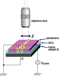
Figure 1: Schematic image of the organic field-effect transistor (OFET) device and its electrical connections.
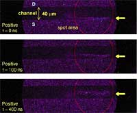
Figure 2: SHG image from the OFET channel for different delay times, applying a positive pulse to the source.
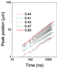
Figure 3: The peak position of the SHG intensity versus time in log-log scale. The applied gate voltages are -20V (squares), -30V (circles), -40V (upward-pointing triangles), -50V (downward-pointing triangles), and -60V (diamonds). The slopes of the fitted lines are listed.