


Tokyo Tech News
Tokyo Tech News
![]()
Published: August 31, 2011
Amorphous oxide semiconductors (AOSs) were developed in 2004 by Kenji Nomura, Toshio Kamiya, Hideo Hosono and colleagues. The demonstrated performance of thin film transistors (TFTs) 1 using (AOSs) is 10 times higher than current amorphous Si TFTs, suggesting the potential of the new material in flat panel displays2.
Electronic devices require very uniform and stable operation characteristics. This is particularly challenging for organic-LED displays, which must have a threshold voltage shift well below 0.1 V. Light illumination, a typical condition for operating flat panel displays, also makes device stability hard to achieve.
Now, Toshio Kamiya, Kenji Nomura, Hideo Hosono and their students at the Materials and Structures Laboratory, Tokyo Institute of Technology, have unveiled details of the electron transport mechanisms, atomic and electronic structures, and several modes of defects and impurities in AOSs that are related to instability issues.
They fabricated amorphous In-Ga-Zn-O TFTs with an Y2O3 passivation layer. Using hard X-ray photoemission spectroscopy they found that the amorphous In-Ga-Zn-O layers have high-density deep defect states near the top-most surface, and these cause instability under illumination with visible light. Forming the passivation layer eliminated these defects, producing highly-stable TFTs with a negligible threshold voltage shift for visible light illumination under bias tests3.
These results point out the importance of deep defects in AOSs, and assist commercialization of high-performance flat panel displays including organic LEDs and flexible displays.
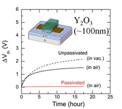
High stability is obtained for an Y2O3-passivated amorphous In-Ga-Zn-O thin-film transistor.
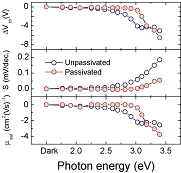
Y2O3 passivation improved the threshold photon energy for instability due to light illumination.
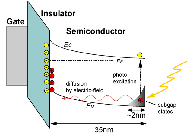
A model of the negative-bias light-illumination instability.
Reference
Toshio Kamiya
Materials and Structures Laboratory
Professor

![]()
© Tokyo Institute of Technology. All rights reserved.
![]()