Any network that transfers information, such as the internet, requires a complicated system of switches and routers to ensure that all the pieces of information, known as packets, reach their correct destinations. One promising new switch design, called an optical packet switching system (OPS) has the potential to operate at high speeds over 40 Gbps (Gigabit per second), and consumes very little power because it eliminates the need to convert between optical and electrical signals.
However, one major hurdle in OPS development is to find an efficient way of processing the packet labels, which contain information on what the data packet contains and where it should go. Generally, the label processing takes up a large percentage of the total power consumption.
Now, Kengo Sawada and Hiroyuki Uenohara from the Precision and Intelligence Laboratory in Tokyo Institute of Technology’s Photonics Integration System Research Centre have developed an optical digital-to-analog converter (ODAC) that can operate at 40 Gbps, and can be applied to label processing in an OPS.
The ODAC is a semiconductor waveguide-based device just 2.5 micrometers wide and 3.5 micrometers deep, with a 0.5 micrometers-thick core of indium gallium arsenide phosphide sandwiched between lower and upper cladding layers of indium phosphide. It also has input and output couplers and a one-bit delay line 2.5 millimeters in length. The intensity of two interfering adjacent bits can be recognized with low-speed electrical comparators after converting the signal from optical to electrical.
The researchers used their device to recognize two-bit optical labels in an input optical packet containing a 40 Gbps, pseudo-random bit sequence signal. Then they showed it was possible to recognize the label information with low-speed electrical comparators after optical-to-electrical conversion. Finally, the control signal of the optical switch could be read out from the electrical address table by using the recognized label information. By this method, input optical packets were properly transferred to the destination output ports.
The study raises hopes that semiconductor integration devices such as ODAC could be used in the near future as high-speed and low-power components for optical network node systems.
Reference
- Authors: K. Sawada, and H. Uenohara.
- Title of original paper: High-Speed Optical Label Recognition Technique using an Optical Digital-to-Analog Conversion and Its Application to Optical Label Switch.
- Journal, volume, pages and year: Journal of Lightwave Technology, 28, No.13, pp.1889-1896 (2010).
- Digital Object Identifier (DOI): 10.1109/JLT.2010.2049339
- Affiliations: Precision and Intelligence Laboratory, Photonics Integration System Research Centre, Tokyo Institute of Technology.
- Department website: http://vcsel-www.pi.titech.ac.jp/index-j.html

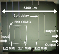
The optical digital-to-analog converter developed by Sawada and Uenohara.