Scientists at Tokyo Tech have developed a new type of transistor made from diamond that could prove valuable for high power applications
Transistors are electronic switches that control the flow of current from one part of a circuit to the next, and form the foundations of modern computing. Transistors are usually made from semiconductors – materials that allow electric current to flow through them only under certain controllable circumstances. Current research is looking into the possibility of using doped diamond as semi-conductors in order to create hard-wearing transistors with a wide band gap, high thermal conductivity and the ability to withstand high electric fields without breaking.
Now, Mutsuko Hatano and co-workers at Tokyo Institute of Technology, together with colleagues across Japan, have succeeded in fabricating a new design of transistor using diamond doped with phosphorus and boron1. The new transistor operates accurately at high temperatures and can prove useful in power devices.
“Naturally, diamond is an insulator,” explains Hatano. “However it becomes semi-conducting when doped with boron or phosphorus. We and our co-workers at the National Institute of Advanced Industrial Science and Technology discovered a unique way of selectively growing doped diamonds. We applied this technique to fabricate diamond junction field-effect transistors.”
Junction field effect transistors (JFETs) work by altering the conductivity of the channel through which the current flows. Each transistor has a drain, source, and gate. The state of the gate (either ‘on’ or ‘off’) determines the current flowing through the channel between the source and the drain. Rather like pinching or squeezing a hosepipe to prevent water flowing, JFETs allow the channel to remain open (on state) or closed (off state).
Hatano and her team built up JFETs by doping diamond with impure gases containing either boron or phosphorus during the chemical vapor depositionprocess. Phosphorus has five free electrons as opposed to diamond’s four, so every atom effectively adds an extra electron (n-type doping). Boron, on the other hand, has only three electrons so every atom creates a ‘hole’ (p-type doping).
The team created the desired shape and structure of each transistor. The flow channel was made up of p-type diamond, with the n-type diamond making a unique structure of two gates placed on either side of the channel.
When open, the p-type channel is full of holes, meaning there is plenty of space for the holes in the current to flow. However, once a voltage is passed simultaneously through the n-type gates, the holes are filled in to create a depletion layer that closes off the channel to current.
The flow of current can therefore be carefully controlled according to the voltage passing through the gates. This is the first transistor of its kind to be made from diamond, and to function accurately even at higher temperatures. The ability of the lateral-gated diamond transistors to withstand high currents and high voltages when stacked vertically means the new devices could be very valuable in power applications.
“The present work is still just the first step,” explains Hatano. “We are going to evaluate and improve the device characteristics. At present, diamond substrates are expensive to use as a power device on a large scale. This will be solved if diamond is grown on another, cheaper substrate in future.”
Reference
- 1 Takayuki Iwasaki et al. Diamond junction field-effect transistors with selectively grown n+-side gates.Applied Physics Express 5 (2012)
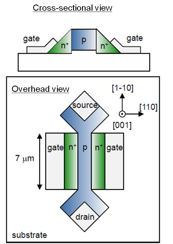
Device structure of the junction FET.
A p-channel is sandwiched by the n+-type diamonds which act as side gates to control depletion layers in the p-channel
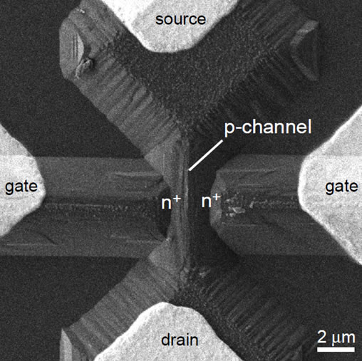
SEM image of diamond JFET with a channel width of 0.5 μm.
The center of the image is the p-channel. The inclined regions next to the p-channel are selectively grown n+-type diamonds continuous to the gate electrodes.
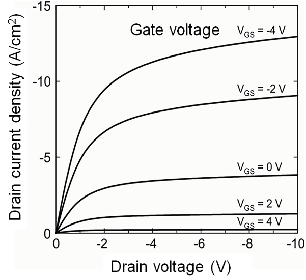
Output characteristics of the junction FET.
The device shows the transition from the linear to the saturation region. The drain current is modulated by the gate voltage.