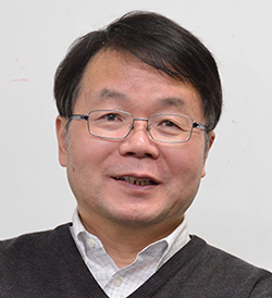
Professor Hideo Hosono has received the Harushige Inoue Award.
The Harushige Inoue Award was instituted to commemorate the 15th anniversary of the establishment of the Research Development Corporation of Japan, one of the predecessors of the Japan Science and Technology Agency (JST), to honor its first president, Harushige Inoue, and his contribution to the development of scientific technology in Japan. Inoue was also the first secretary of the Agency of Industrial Science and Technology.
- Research topic
"Development of a sputtering target of oxide semiconductor In-Ga-Zn-O"
- Researcher
Professor Hideo Hosono
Materials and Structures Laboratory, Tokyo Institute of Technology
- Developing company
Shigeru Oi, President and Chief Executive Officer, JX Nippon Mining & Metals Corporation
(Nominated by Akihito Suzuki, Unit Chief, Electronic Materials Group, JX Nippon Mining & Metals Corporation)
This technology is regarding the target material for the oxide semiconductor In-Ga-Zn-O (Indium Gallium Zinc Oxide, "IGZO"), used in the semiconductor layer of thin film transistors (TFT), which drives the pixel electrodes of flat panel displays.
Professor Hideo Hosono independently proposed design guidelines for transparent amorphous oxide semiconductors (TAOS) with high electron mobility in 1995. In 2004, he produced a TFT with an active layer of IGZO (a kind of TAOS) on a substrate of plastic, and reported in Nature that a high mobility of approximately 20 times the conventional amorphous silicon could be attained. This paper was the first to show that a high-performance TFT could be made easily with oxide semiconductors. It focused the attention of many companies, inside and outside Japan, on IGZO and triggered research and development toward the commercial use of IGZO-TFT.
In this climate, JX Nippon Mining & Metals researched the development of a target material which is of high purity and high density, and has a microstructure which is fine and uniform. In 2011, ahead of other companies, it succeeded in mass-producing a large sputtering target (2.7 m in length) which, for the first time, could be used with 8.5th-generation film-forming equipment.
Panel manufacturers inside and outside Japan used the target material produced by JX Nippon Mining & Metals, and confirmed that low-defect IGZO thin film could be produced at a high yield. The practical application of displays using IGZO-TFT began in earnest. Displays using IGZO-TFT are highly acclaimed for their characteristics, including high definition and low power consumption, and are expected to claim more market share in the future. Additionally, IGZO-TFT is anticipated to be applied to organic electroluminescence displays and flexible displays. The importance of development of IGZO target materials for the front end of the manufacturing process is increasing accordingly.
Comment from Professor Hideo Hosono
Our papers about crystalline IGZO-TFT were first published in Science in 2003, and those about amorphous IGZO-TFTs in Nature in 2004. Prior to that, we had already applied for patents by JST which was the sponsor of the project. To utilize IGZO-TFT to drive a display, a large, dense ceramic target is necessary to form a homogeneous thin film on a large-sized substrate glass by sputtering. The co-recipient of this award, JX Nippon Mining & Metals, was the first to perfect this technology, and the tangible result was displayed at an international workshop hosted by Tokyo Tech in 2010 (TAOS 2010). This let the attendees know that we were on course for practical use. Also, they were the first to license the patent and succeeded in applying it commercially. Since then, many companies inside and outside of Japan have followed. I pay my respects to the high technology and morals of this company.
. Any information published on this site will be valid in relation to Science Tokyo.


