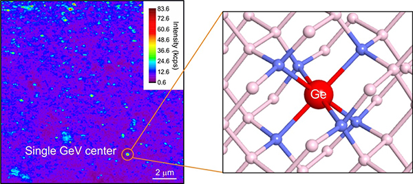
Germanium defects in a diamond crystal lattice act as a reliable source for single photons, new research shows. The results are reported in Scientific Reports and provide a promising new route to building components for quantum cryptography and biomarkers.
Pure diamonds are naturally colorless, but gaps in the crystal structure or impurities of other elements can create colors and even emit fluorescence. Recently, researchers have shown that the fluorescent lattice defects could be useful as single photon sources for quantum cryptography and as bright luminescent makers in living cells.
Now, Takayuki Iwasaki and co-workers at Tokyo Institute of Technology (Tokyo Tech), together with scientists across Japan and Germany, have demonstrated a new type of diamond crystal defect that fluoresces to produce single photons in a narrow, high energy wavelength band. The defects, which have been named germanium-vacancy (GeV) centres, are relatively easy to fabricate in a reliable, reproducible way.
Iwasaki and co-workers were inspired by recent work that demonstrated fluorescence from nitrogen-vacancy (NV) and silicon-vacancy (SiV) defects in diamond. They used an ion implantation method to insert germanium atoms into diamond films, before heating the films at 800 °C. The resulting samples showed fluorescence only after heating, which induces diffusion of vacancies in the diamond lattice. The researchers therefore concluded that the fluorescence was produced by combined defects, each comprising a germanium atom side-by-side with a vacancy.
The GeV centres produced single-photon bursts of fluorescence centred at a wavelength of around 602 nm, representing a higher energy fluorescence than SiV centres. Moreover, the researchers were also able to create the films through the less destructive method of chemical vapor deposition, producing films with narrower and more stable emission peaks of ensemble GeV centres which are useful for biomarkers.
Overall, the work opens up a promising new avenue for developing sources of single photons, which are essential for quantum cryptography. Iwasaki and co-workers are also hopeful that they could incorporate GeV centres in nanodiamonds for use as biological markers.
Background
Quantum computing and cryptography
Our current digital computers encode information in bits, which can have values of either 0 or 1. In quantum computers, data will instead be stored in 'qubits', which can take on values of not only 0 or 1, but also a superposition of the two states. This small difference represents a huge change in functionality, and allows information and data to be encrypted in ways that are impossible to decode using only classical methods-this is known as quantum cryptography. Indeed, quantum-encoded data cannot be copied or read without changing its state, meaning that it is impossible for third parties to eavesdrop on communications without being discovered.
Single photon generation
To achieve the secure data transmission by quantum cryptography, individual photons of known wavelengths must be used but are difficult to generate. Herein lies the motivation behind the work of Iwasaki and co-workers. Defects in diamond have been shown to produce fluorescence — emitting photons of fixed-wavelength light when illuminated by higher energy light — but these are often unreliable or difficult to fabricate. The search is on for new defect structures that not only produce strong, consistent fluorescence, but can also be made in a reproducible way.
Biomarker
To monitor individual proteins and the interior of living cells, nanometer sized markers such as fluorescent proteins and quantum dots are used. Due to the high biological compatibility of diamond, fluorescent defects in diamond nanostructures are stable biomarkers without optical bleaching. The bright emission from the GeV centres could be suitable for such biological applications.
Methodology
Iwasaki and co-workers began with an ion implantation method, which involved firing germanium atoms at high speed into pure diamond surfaces. They then heated the samples at 800 °C to induce diffusion of vacancies — gaps in the diamond crystal lattice where a carbon atom is missing. By using Raman spectroscopy and confocal microscopy they observed fluorescent light emerging from the samples at a wavelength of around 602 nm. The team used theoretical calculations to deduce that this fluorescence resulted from combined defects, each comprising a germanium atom next to a lattice vacancy.
The biggest step forward in the work was when Iwasaki and co-workers managed to create the same types of defects through a different method, microwave plasma chemical vapor deposition (MPCVD). MPCVD involves reactions of volatile chemicals on a substrate, and is often used to make synthetic diamonds. The defects in the sample prepared using MPCVD gave off more consistent fluorescence with a narrower and more stable peak. Moreover, MPCVD provides closer control over the fabrication process, and is less likely to produce unwanted damage to the samples than ion implantation.
Future work
Further work is needed to refine the fabrication process so that diamond films with germanium defects could be incorporated into devices for reliable single photon generation on demand.

Figure. Single GeV center in diamond. (left) Fluorescence mapping and (right) atomic structure model.
Reference
Authors: |
Takayuki Iwasaki, Fumitaka Ishibashi, Yoshiyuki Miyamoto, Yuki Doi, Satoshi Kobayashi, Takehide Miyazaki, Kosuke Tahara, Kay D. Jahnke, Lachlan J. Rogers, Boris Naydenov, Fedor Jelezko, Satoshi Yamasaki, Shinji Nagamachi, Toshiro Inubushi, Norikazu Mizuochi and Mutsuko Hatano |
Title of original paper: |
Germanium-Vacancy Single Color Centers in Diamond |
Journal: |
Scientific Reports |
DOI : |
|
. Any information published on this site will be valid in relation to Science Tokyo.


