Tokyo Tech and Fujitsu Achieve Wireless Transmission Speeds of 56 Gbps, World's Fastest
—Millimeter-waveband wireless device implemented in CMOS integrated circuit—
Tokyo Tech and Fujitsu Laboratories Ltd. announced on February 1 that, in an effort to further enlarge the capacity of wireless equipment, they have developed a CMOS wireless transceiver chip that can process signals at high speeds with little loss across a broad range of frequencies, from 72 to 100 gigahertz (GHz). They also developed technology to modularize it. With these developments, they succeeded in achieving wireless transmission speeds of 56 Gigabits per second (Gbps), the world's fastest.
In recent years, to cope with the large increase in data traffic resulting from the widespread use of smartphones and other devices, networks that link base stations use optical fiber. One issue with this approach, however, is that it is difficult to expand service in areas where it is difficult to install a network of optical fiber cables, such as in urban areas or areas surrounded by rivers or mountains. To deal with this issue, Tokyo Tech and Fujitsu Laboratories have now developed high-speed wireless transceiver technologies that uses the millimeter-waveband (30&8211;300 GHz), where there are few competing wireless applications, and which is capable of large-capacity communications.
This technology makes it possible to have high-capacity wireless communications equipment that can be installed outdoors in applications where fiber-optic networks would be difficult to lay.
The details of this technology will be announced at the IEEE International Solid-State Circuits Conference 2016 (ISSCC 2016), the largest conference related to semiconductor technology, opening in San Francisco on January 31 (ISSCC Presentation Number 13.3).
Background
With sharp increases in data communications traffic resulting from the proliferation of smartphones, the expansion in the capacity of backbone networks—which connect wireless base stations to core networks, and base stations to each other—is accelerating. In the past, macro-cell base stations were mainly used, each of which can cover an area with several kilometers of range, but in recent years these have been supplemented with large quantities of small-cell base stations, each of which has a range of only a few hundred meters, to accommodate the increase in communications traffic.
Also, fiber-optic lines, which can transmit large volumes of data, are currently the most common way to handle communications between base stations. But laying new fiber-optic cables can be difficult in tightly packed urban areas, or in places hemmed in by mountains or rivers, so it has been hoped that high-capacity wireless equipment could be created that can easily be installed outdoors.
Issues
High-capacity wireless transmissions need to use broad frequency ranges. This makes the use of the millimeter-waveband a suitable option, as few competing wireless applications use it. But because the millimeter-waveband uses such high frequencies, designing CMOS integrated circuits for that purpose has been a challenge, as the circuits need to be designed to operate near their limits. It has also been difficult to develop low-loss transceiver circuits that modulate and demodulate broadband signals into and out of the millimeter-waveband with high quality, and low-loss interface circuits, which connect the circuit board to the antenna.
About the Technology
The newly developed CMOS wireless transceiver chip and the wireless module that includes it (Figure 1) are comprised of two key technologies.
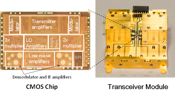
Figure 1. Transceiver CMOS chip and module.
1. Low-loss, high-bandwidth transceiver circuit
Tokyo Tech developed a technology for broadband, low-loss transceiver circuits in which data signals are split in two, with each converted to different frequency ranges, and then recombined (Figure 2). Each signal is modulated into a band 10-GHz wide, with the low-band occupying the 72–82 GHz range, and the high-band occupying the 89–99 GHz range. This technology enables modulation on an ultra-wideband signal of 20 GHz, with low noise and a similar range in the ratio between input and output power as existing 10 GHz band methods, which results in high-quality signal transmissions.
Tokyo Tech also developed an amplifier to send and receive as radio waves signals converted to the millimeter-waveband. The ultra-wideband amplifier for 72 to 100 GHz was designed with circuit technologies that stabilize the amplification ratio by feeding the amplitude of the output signal back to the input side for signal components whose amplification ratio decreases based on frequency.
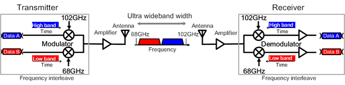
Figure 2. Transceiver configuration.
2. Modularization technology
The signal converted to the millimeter-waveband by the semiconductor chip is transported over the circuit board's signal path and supplied to the antenna. Because the antenna is made out of a waveguide (a metallic cylinder), there needs to be an ultra-wideband, low-loss connection between the printed circuit board and the waveguide. Fujitsu Laboratories and Tokyo Tech developed an interface between the circuit board and waveguide that uses a specially designed pattern of interconnects on the printed circuit board to adjust the impedance for the ultra-wideband range, enabling loss in the desired frequency range to be greatly reduced.
In this development project, Tokyo Tech was primarily responsible for reducing transceiver-circuit losses and developing broadband technologies, while Fujitsu Laboratories mainly handled modularization technologies.
Results
Indoor data-transfer tests were conducted, with two modules facing each other separated by a distance of 10 cm. These tests achieved data-transfer rates of 56 Gbps, the fastest wireless transmission speeds in the world, with loss of maximum 10% between the waveguide and circuit board.
By combining the technologies developed in this project with high-output amplifier technology, used to amplify the signal and increase the transport range, and baseband-circuit technology, used to process ultra-wideband signals, it is possible to increase the capacity of wireless equipment that can be installed outdoors. By doing so, even in places where new fiber-optic lines are difficult to install, such as urban areas and places surrounded by mountains or rivers, a high-capacity wireless base station network can be deployed, thereby contributing to the provision of a comfortable communications environment in those places.
Future Plans
Fujitsu Laboratories aims to have a commercial implementation of wireless trunk lines for cellular base stations around 2020.