AGC starts mass-production of sputter target of C12A7 electride created by Tokyo Tech.
Thin films of C12A7 electride contribute to fabrication of large-sized, efficient organic EL panels.
Tokyo Tech and AGC Asahi Glass (AGC) have developed a uniform amorphous thin film of C12A7 Electride, which was developed by a study group of Professor Hideo Hosono at the Tokyo Tech, and AGC has started commercial production of a sputtering target material needed to mass-produce the thin film.
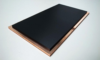
Figure1: Photo of sputtering target of C12A7 Electride
C12A7 is a component of alumina cement. It has a structure of interconnected cages (about 0.4 nm[1] in inner diameter), which contain oxygen ions. By replacing all of the oxygen ions in the cages with electrons, the study group of Professor Hosono developed C12A7 Electride, which readily conducts an electric current like a metal, is stable chemically and thermally, and is easy to handle, while having the characteristic of readily emitting electrons. The study group also demonstrated that it can manufacture amorphous C12A7 Electride, which it found maintains the characteristics of C12A7 Electride.
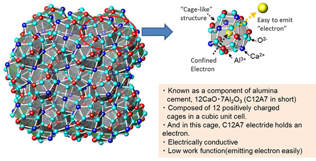
Figure2: C12A7(12CaO・7Al2O3) crystal structure
Currently, lithium fluoride (LiF) and alkali-doped organic materials are used as the electron injection material for an organic EL display. However, these materials are unstable and are used in an unstable state. Accordingly, the study group of Professor Hosono and the AGC Group developed the amorphous C12A7 Electride thin film, which is more stable. The amorphous C12A7 Electride thin film, which can be formed through a sputtering process[2] at room temperature using the AGC Group-developed target material, has the following unique characteristics: it is transparent in the visible range; it can emit electrons as easily as metal lithium can; and it is chemically stable even in the atmosphere.
By combining this with an n-channel TFT element, which uses a transparent amorphous oxide semiconductor TAOS[3]; developed by the study group of Professor Hosono, the low-driving-voltage electron transport layer can be manufactured stably and with high production yields even in the case of an inverted-structure organic EL display whose structure is advantageous for a device.
TAOS-TFT is suitable for driving a large organic EL panel, but there was no material that functions properly as an electron injection layer and an electron transport layer, which are necessary to realize an inverted structure that makes the best of the panel's performance. A series of these achievements is expected to substantially improve production of oxide TFT-driven organic EL panels.
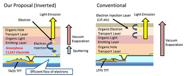
Figure3: OLED device structure.
The stacking order of each layer in the left is the reverse of the conventional one.
Program Information
A part of this achievement has been made in pursuing the following R&S topic of the ACCEL
- ACCEL : Strategic Basic Research Program of Japan Science and Technology Agency (JST)
- Topic : "Materials Science and Industrial Application of Electride." (2013-2018)
- Research Director : Hideo Hosono (Tokyo Tech)
- Program Manager : Toshiharu Yokoyama
- Collaborating research institutes : AGC Asahi Glass
Explanations of Technical Terms
1.nm
1/1000 micron
2. Sputtering process
Sputtering is a process whereby particles are ejected from a solid target material due to bombardment of the target by energetic particles. Because the principle is simple and various sputtering devices are available, this method is used widely in various technical areas. Recently, the method has been used to manufacture thin films for semiconductors, LCDs, plasma displays, and optical discs, for which high-quality thin films are needed.
3. TAOS
TAOS stand for transparent amorphous oxide semiconductor. IGZO is one of TAOS's and composed of In-Ga-Zn-O. This terminology was first introduced in 1996 by Hosono Group.