Understanding how shock waves affect structures is crucial for advancements in material science research, including safety protocols and novel surface modifications. Using X-ray diffraction probes, scientists at the Institute of Materials Structure Science of KEK, Tokyo of Tech, Kumamoto University, and University of Tsukuba studied the deformation of polycrystalline aluminum foil when subjected to a laser-driven shock wave.
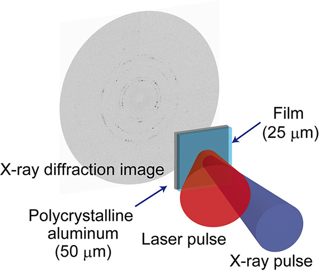
Figure 1. Diffraction patterns of deformed crystals
Aluminum foil irradiated by a laser-driven shock wave is followed by an X-ray pulse to read the diffraction pattern of the crystal structure.
The foundations of engineering lie in understanding and manipulating the structure of materials to harness their properties in creative ways. Interactions between materials take place via the exchange of forces so predicting a material's ability to withstand a force and how it propagates is central to developing structures with enhanced strength.
If an instantaneous strong force acting on a material results in a shock wave, the atoms may become displaced or dislocated. Like a rubber band, if the external force is not too significant, the internal forces can resist and the material can return to its original state (elastic deformation). But beyond a certain limit, the force may result in permanent damage or even structural failure (plastic deformation) of the material.
Unit cells are the smallest regularly repeating three dimensional atomic structure that reflects the overall symmetry of a crystal, and studying their displacement can provide rich insights. However, observing processes at the atomic scale is very difficult. This is where x-ray diffraction comes to the rescue. Envision a camera that allows you to capture events taking place at the atomic scale. When an x-ray encounters an atom it gets absorbed and then re-emitted by the atom. This results in the wave being scattered or diffracted in an orderly fashion, owing to the orderly arrangement of atoms in the crystal. Depending on the size, spatial arrangement, and distance between the atoms, the wave is scattered in different directions with different intensity. Thus, the atomic structure is captured as signals, like a photograph of the crystal during and after the shock wave passes. This can be used to decode crystal deformation.
Motivated by this, researchers conducted an experiment to observe the deformation process of polycrystalline aluminum foil when subjected to a laser-driven shock wave. This disturbance was then captured as diffraction spots of an x-ray beam which could be simultaneously compared to the diffraction pattern of the pre-shock crystal (Fig. 1). They found that large grains of aluminum were rotated, compressed elastically, and reduced in size along the wave direction. As the wave propagated deeper into the sample, the diffraction spots smoothed and broadened, and the original diffraction spots began to disappear, replaced by a new set of spots (Fig. 2). "We observed grain refinement and structural changes of the polycrystalline metal, which increased with the propagation of the laser-driven shock wave. This, in turn, enabled the study of microstructural deformation in plastic shock flows from the atomic to the mesoscale level," stated Dr. Kohei Ichiyanagi of High Energy Accelerator Research Organization and Jichi Medical University.
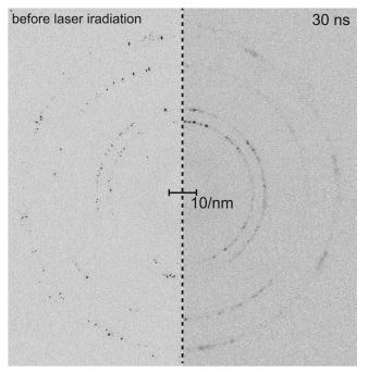
Figure 2. Pre and post shock wave diffraction pattern of crystals
Diffraction images of polycrystalline aluminum foil before laser irradiation (left image) and after shock wave propagation (right image). The laser-induced shock wave pattern is smoothed due to plastic deformation.
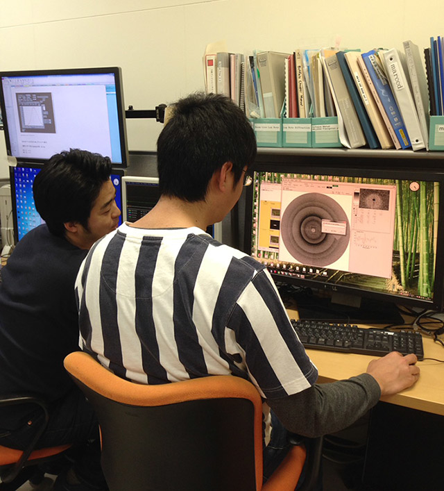
Researchers working in the control room
Kouhei Ichiyanagi (left) and Sota Takagi, Doctoral student of University of Tsukuba analyzed the diffraction images of the pre- and post-shocked samples.They irradiated the samples with 100 picosecond X-ray pulses synchronized during one high intensity pulsed laser irradiation (8 nano sec), changed the irradiation timing by 3 nano sec and shot the image repeatedly,then succeeded in acquiring time-resolved diffraction images.
Contemporary research of post-shock structural changes of materials often fails to highlight the process of wave dissipation and the distribution of defects. This research changes the status quo by providing a method to observe grain refinement and structural changes, including surface hardness and modification, of polycrystalline metal during shock wave loading. Optimistic about the potential of this research, Professor Kazutaka G. Nakamura of the Tokyo Institute of Technology said, "Our technique will be valuable for revealing mechanisms of microstructural change for various alloys and ceramics based on dynamic processes."
Surely, this goes to show the creative ways we can expand the reaches of what we are able to see: this time, it's how x-rays can be used to capture how particles are shaken and stirred!
Reference
Authors : |
Kouhei Ichiyanagi1,2, Sota Takagi2,3, Nobuaki Kawai4, Ryo Fukaya2, Shunsuke Nozawa2, Kazutaka G. Nakamura5, Klaus-Dieter Liss6,7, Masao Kimura2 & Shin-ichi Adachi2 |
Title of original paper : |
Microstructural deformation process of shock-compressed polycrystalline aluminum |
Journal : |
Scientific Reports |
DOI : |
|
Affiliations : |
1Division of Biophysics, Department of Physiology, Jichi Medical University Japan.
2Photon Factory, Institute of Materials Structure Science, High Energy Accelerator Research Organization, Japan.
3Division of Earth Evolution Science, Graduate School of Life and Environmental Sciences, University of Tsukuba, Japan.
4Institute of Pulsed Power Science, Kumamoto University, Japan.
5Laboratory for Materials and Structures, Tokyo Institute of Technology, Japan.
6Materials and Engineering Science Program, Guangdong Technion-Israel Institute of Technology, China.
7Technion-Israel Institute of Technology, Israel.
|