Tokyo Institute of Technology President Kazuya Masu (research director, JST-CREST project in Nano-electronics) and NTT Advanced Technology Corporation succeed in the development of high-sensitivity and low-noise MEMS1accelerometer by using multi-layer metal structures that are composed of multiple metal layers. The developed accelerometer achieves 1 µG level resolution that has been a challenging task with conventional MEMS technology. (G: gravitational acceleration, G = 9.8 m/s2) The proposed technology is an innovative solution to increase the resolution of miniaturized accelerometers for general purpose use. Such accelerometers would be useful for the development of new devices and systems for medical and healthcare system, infrastructure monitoring, mobile vehicle control and robot technology that require motion sensing. The research group has previously proposed a method of using gold material to downscale the proof mass size of MEMS accelerometers to less than one-tenth. Expanding this achievement, in this work, they have increased the proof mass per area by employing multiple layers of gold for the MEMS structures, and thereby successfully increasing the sensitivity over one hundred times and reducing noise less than one-tenth when compared with conventional ones.
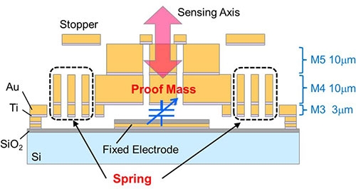
Figure 1. Schematic image of the proposed MEMS structure.
The illustration shows a schematic image of the proposed single-axis MEMS capacitive accelerometer. Input acceleration can be sensed by monitoring the capacitance change between the proof mass and the fixed electrode. The device is realized by the multiple layers made of electroplated gold. We utilize the third (M3) and fourth (M4) layers for the spring structure, and the M4 and fifth (M5) layers for the proof mass structure.
A significant increase in the demand of accelerometers is expected as the market for consumer electronics, such as smartphones, and social infrastructure monitoring applications are expanding. Such miniaturized and mass-producible accelerometers are commonly developed by silicon MEMS technology where the fabrication process is well established.
In the design of accelerometers, there is a trade-off between the size reduction and the noise reduction because the mechanical noise dominated by the Brownian noise is inversely proportional to the mass of the moving electrode called as proof mass. Moreover, as for capacitive accelerometers, the sensitivity is generally proportional to the accelerometer size, and thus there is also a trade-off between the size reduction and the sensitivity increase. Since high-resolution accelerometers require low noise and high sensitivity performances, it has been difficult for conventional silicon-based MEMS accelerometers to detect 1 µG level input acceleration.
Low noise and high sensitivity MEMS accelerometer
The research group consisting of Tokyo Tech and NTT Advanced Technology Corporation has previously proposed a method to downscale the proof mass size of MEMS accelerometers to less than one-tenth by using gold material. In this work, as an extension of this achievement, they have employed multi-layer metal structures to the proof mass and spring components, and developed a low noise and high sensitivity MEMS accelerometer.
As shown in Fig. 1, they reduced the Brownian noise being inversely proportional to the proof mass by increasing the mass per area with the use of multiple layers of gold for the proof mass structure.
Furthermore, they utilized the whole area of the 4 mm square chip by reducing the warpage of the proof mass, which enabled them to increase the capacitance sensitivity of the accelerometer. Figure 2 shows a chip photograph and scanning electron microscope images of the developed MEMS accelerometer.
With these results, the developed accelerometer achieved the sensitivity to be one hundred times or more and the noise to be one-tenth or less as compared with conventional accelerometers with the same size, as shown in Fig. 3. Accordingly, they confirmed that the accelerometer would have potential to detect input acceleration to be as low as 1 µG. The fabrication process utilized semiconductor microfabrication process and electroplating, and thus it could be possible to implement the developed MEMS structures on an integrated circuit chip. Therefore, the proposed technology would be useful to increase the resolution of miniaturized accelerometers for general purpose use.
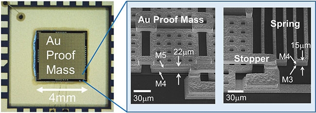
Figure 2. Photographs of a developed device.
Left; The photo shows a developed high-sensitivity MEMS Accelerometer. The Au proof mass was fabricated on a silicon die. The accelerometer was implemented in a ceramic package and wire-bonded. Right; The SEM images show the close-up views of the Au proof mass and the spring structure. The Au proof-mass structure of 22-μm thickness was successfully developed by employing the M4 and M5 layers. The serpentine spring structure was made of the M3 and M4 layers. The serpentine springs and stoppers were placed at each corner of the proof mass.
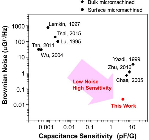
Figure 3. Performance comparison.
The graph shows a comparison of Brownian noise (BN) versus capacitance sensitivity. Thanks to the high density of gold, the BN achieved in this work was more than an order of magnitude lower than those of conventional devices when compared with the same sensitivity. Furthermore, our device was fabricated by surface micromachining that would useful for miniaturization.
An era of placing a large number of sensors on all thing
It would be a breakthrough in a variety of motion sensing application to realize an ultra-compact and high-resolution accelerometer. Such accelerometer can be applied to medical and healthcare technology, infrastructure monitoring, high precision control of ultra-lightweight robots, mobile vehicle control, navigation system in places where GPS cannot be used and space environment measurement that needs ultra-low acceleration sensing.
In the near future, an era of placing a large number of sensors on all thing is expected to come, and in such case, it would be extremely important to miniaturize high-resolution accelerometers because accelerometer technology is a fundamental of motion sensing.
Reference
Authors : |
Daisuke Yamane1, Toshifumi Konishi2, Teruaki Safu2, Hiroshi Toshiyoshi3, Masato Sone1, Katsuyuki Machida1, Hiroyuki Ito1, and Kazuya Masu1 |
Title of original paper : |
A MEMS Accelerometer for Sub-mG Sensing |
Journal : |
Sensors and Materials |
DOI : |
|
Affiliations : |
1Tokyo Institute of Technology, Japan
2NTT Advanced Technology Corporation, Japan
3The University of Tokyo, Japan
|
1 MEMS (Microelectromechanical Systems)
A term that represents micrometer-scaled three-dimensional electronics and mechanical devices manufactured by semiconductor microfabrication process. Currently, the majority of commercialized accelerometers are silicon-based MEMS devices.
- *
- This article has been updated to add information to the reference on October 2.