Nippon Telegraph and Telephone Corporation (NTT) and Tokyo Institute of Technology (Tokyo Tech) have demonstrated an ultrafast all-optical switching operation with the lowest energy consumption ever reported for all-optical switching at less than one picosecond (one trillionth of a second). Previously reported all-optical switches would have difficulty operating at such a high speed with low energy consumption. The current achievement combines an ultrasmall optical waveguide with a height and width of a few dozen nanometers, called a plasmonic waveguide1, with graphene2, a material that shows great promise for nonlinear optics. Such ultrahigh switching speed cannot be achieved by electrical control. It is expected that this switch will be used in future photonic integrated circuits for ultrafast information processing. In addition, this development shows novel promising possibility for applications of plasmonics.
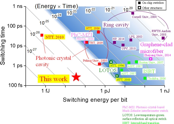
Figure 1. Performance comparison of various all-optical switches.
Background
Optical switches will be important components in future photonic integrated circuits for ultrafast information processing. Optical switches control the on/off state or the direction of optical signals, and the switching speed depends on whether the optical signals are optically or electrically controlled. All-optical switches control optical signals with other optical signals, so they are unaffected by the RC time constant3, which limits the operation speed of electrical devices. Thus, it has been expected that all-optical switches will operate faster than electrically controlled ones. However, the switching energies of the previously reported all-optical switches are relatively large. This energy problem is a critical one for ultrafast information processing because optical components must be densely integrated in photonic circuits and the energy consumption of each device must be low. As shown in Fig. 1, high speed and low energy consumption have not been achieved simultaneously with the previously reported all-optical switches, and it had been assumed that a trade-off existed between the switching energy and switching time. In 2020, however, NTT overcame this trade-off and demonstrated all-optical switching with an extremely small driving energy by using a photonic crystal nanocavity with modest operating speed (tens of picoseconds). On the other hand, the trade-off still remained in the ultrafast switching regime (less than one picosecond), which is beyond the capability of electrical control.
Achievements
NTT and Tokyo Tech developed an all-optical switch operating in the ultrafast regime (less than one picosecond) with low energy consumption by combining an extremely small optical nanoscale waveguide based on plasmonics4 with graphene (Fig. 2a). The main points are as follows.
To control optical signals with other optical signals, the properties of a material placed on the optical path must be changed with light, and the response time (i.e., the time in which this change occurs) is the one of the limitations on the switching time. Here, we employed graphene, which has an ultrafast nonlinear optical response. Graphene is not only a promising for its speed; it also has a large absorption coefficient6 over a broadband wavelength range. On the other hand, graphene is only one-atom thick, and the interaction with light is weak, which leads to long photonic devices and high energy consumption. In this work, we overcame this problem by strongly confining light within a nanoscale plasmonic waveguide.
We fabricated small plasmonic waveguides with a core size of 30 nm × 20 nm and loaded graphene on them by using NTT's nanofabrication technologies (Fig. 2b). The cross-sectional area of these plasmonic waveguides is about 1/100th that of "compact" silicon waveguides and 1/105 that of single-mode optical fibers. It was experimentally shown that the absorption coefficient of the graphene-loaded plasmonic waveguide is one order of magnitude smaller than that of graphene-loaded silicon waveguides. Moreover, the energy required for inducing nonlinear optical effects is four orders of magnitude smaller. These results show that compactness and low energy consumption can be achieved at the same time.
- Figure 2.
- Schematic (a) and scanning electron microscope image (b) of the graphene-loaded plasmonic waveguide.
2. Demonstration of ultrafast all-optical switching
The signal light is switched (on/off) with control light in all-optical switches (Fig. 3a). In our switch, the control light induces a nonlinear optical effect of graphene; i.e., it changes the degree of absorption by graphene. Figure 3b indicates that a switching time of 260 fs can be achieved with a switching energy of 35 fJ. The switching time is one order of magnitude shorter and the energy four orders of magnitude smaller than those of previous graphene-based devices. In addition, as shown in Fig. 1, the switching energy is the smallest value ever reported (1/100th of that previously reported) for any type of all-optical switch operating at less than one picosecond. Thus, we developed the first all-optical switch operating with a response time in the femtosecond range and an energy consumption in the femtojoule range. Moreover, the energy-time product, which is a measure of the trade-off mentioned above, was somewhat improved over that of the previous best device.
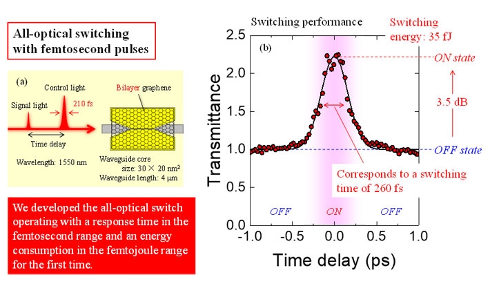
- Figure 3.
- Demonstration of ultrafast all-optical switching: (a) schematic setup and (b) switching performance.
Outlook
NTT and Tokyo Tech are working on overcoming the limitations of electronics, such as on the operation speed and energy consumption, by integrating a dense photonic network into a processor chip. The all-optical switch operates much faster than an electrically controlled one and consumes less energy. We expect that it will be used in future photonic integrated circuits for ultrafast information processing. As well, the nanoscale waveguide of the switch is a superior platform for developing nanophotonic information processing devices incorporating nanowires and other two-dimensional materials. Moreover, we envision that our device can be used as a nonlinear activation function in optical neural networks. In the future, we will increase the performance of the all-optical switch, apply its technology to other photonic devices such as detectors, and examine the use of other nanomaterials.
Technical features
1. Ultrafast nonlinear optical effect in graphene
We employed graphene for ultrafast operation. Monolayer graphene absorbs 2.3% of light over a broadband wavelength range (from visible to infrared), and this value means that graphene has a much larger absorption coefficient than that of conventional semiconductors. In addition, graphene shows saturable absorption7, a nonlinear optical effect, and its response time can be less than 100 fs. This ultrafast response originates from the very short relaxation times of graphene carriers. In our switch, a transmittance change induced by saturable absorption switches the on/off state, and the absorption saturates as a result of photo-excited carriers.
2. Enhancement of the interaction between graphene and light by plasmonics
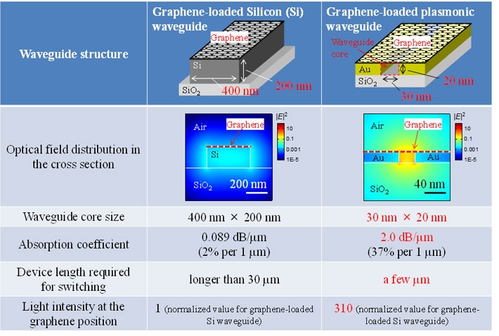
Graphene is a promising nonlinear optical material, but it is too thin to be used in optical devices. Here, we utilized a plasmonic waveguide with a height and width of a few tens of nanometers to enhance the interaction between graphene and light. Plasmonic waveguides strongly confine light—with a core width of only 30 nm and height of only 20 nm, the core area of our waveguide is as small as λ2/4,000 (wavelength λ in this case is 1,550 nm). The interaction between graphene and light is weak when a conventional waveguide made of silicon is used; a numerical calculation gives an absorption coefficient of 0.089 dB/μm (2% per μm) for a graphene-loaded silicon waveguide with a core measuring 400 nm × 200 nm (Fig. 4). This means that a device longer than 30 μm would be needed to obtain 50% absorption. On the other hand, the absorption coefficient for a plasmonic waveguide is estimated to be much higher, 2.0 dB/μm (37% per μm) for a core size of 30 nm × 20 nm, which enables the device length to be decreased. Furthermore, the light intensity at the position of the graphene is 310 times larger than that for a silicon waveguide because the plasmon waveguide core is much smaller. This enhancement significantly reduces the switching energy.
The above enhancement effects were observed in experiments. In particular, the experimentally obtained absorption coefficient for the plasmonic waveguide was 1.7 dB/μm. In addition, the obtained saturation energy was 12 fJ, which is four orders of magnitude smaller than that for graphene-loaded silicon waveguide. Because an increase in light intensity can be regarded as a reduction of the saturation energy in saturable absorption, this result means that the light intensity was enhanced by four orders of magnitude.
- Figure 4.
- Comparison of a graphene-loaded silicon waveguide and a graphene-loaded plasmonic waveguide (simulation).
3. Overcoming the drawbacks of plasmonics with mode converters
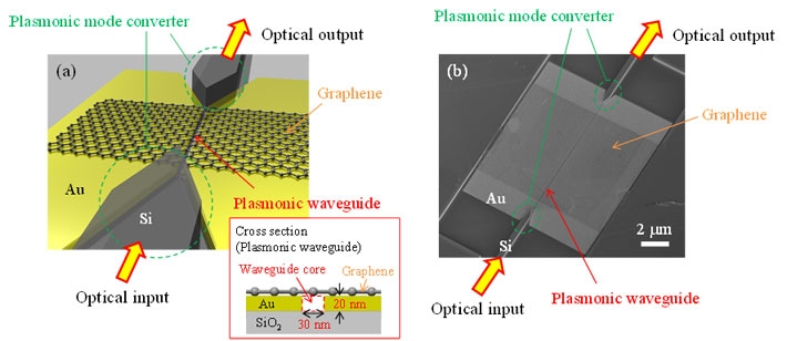
Although plasmonic waveguides strongly confine light, they have a large propagation loss, and directly coupling light to them is not easy because their waveguide cores are much smaller than the wavelength of light. Thus, we utilized the plasmonic waveguides only for the interaction with graphene and used highly efficient plasmonic mode converters to connect the plasmonic waveguides to conventional low-loss dielectric waveguides (Fig. 5). An advanced fabrication technique is needed to make this mode converter; here, NTT developed a plasmonic mode converter connecting a deep-subwavelength plasmonic waveguide and a silicon waveguide in 2016. The plasmonic mode converters enable us to fully enjoy the merits of plasmonic waveguides and graphene in photonic integrated circuits.
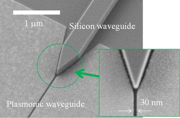
Figure 5. Scanning electron microscope image of the plasmonic mode converter.
1 Plasmonic waveguide
In the vicinity a metal-dielectric interface, light exists in strongly localized coupled states with electrons. Called surface plasmon polaritons, these states can be exploited to make a so-called plasmonic waveguide; light propagates in this waveguide is confined within a nanoscale region around the interface.
2 Graphene
Composed of monolayers of carbon atoms arranged in a hexagonal lattice, graphene has optical and electrical properties that are superior for many purposes because of its unique band structure originating from its low dimensionality.
3 RC time constant
The RC time constant is a measure that indicates how long it takes a certain capacitance to charge to a certain voltage level. It is determined by the product of the resistance (R) and the capacitance (C) in the RC circuit. All-optical devices do not have electric circuits and thus are capable of ultrafast operations not limited by the RC time constant.
4 Plasmonics
Nanophotonics is the study of light in the nanoscale regime, and one of its goals is using light to overcome the limitations of electronics. Plasmonics is one of the research areas in nanophotonics, and involves the study of metal nanostructures, such as plamonic waveguides1, as means of reaching this goal. Plasmonics enables us to confine light beyond the conventional diffraction limit within a nanoscale volume.
5 Nonlinear optical effect
The nonlinear optical effect is one in which a material shows nonlinear response to light intensity when it is irradiated high-intensity light, which induces various phenomena such as saturable absorption.
6 Absorption coefficient
The absorption coefficient shows how well a material absorbs light per unit length.
7 Saturable absorption
The saturable absorption is a phenomenon in which absorption is saturated under high-intensity light irradiation.
Reference
Authors : |
Masaaki Ono1,2, Masanori Hata2,3, Masato Tsunekawa2,3, Kengo Nozaki1,2, Hisashi Sumikura1,2, Hisashi Chiba2,3 and Masaya Notomi1,2,3 |
Title of original paper : |
Ultrafast and energy-efficient all-optical switching with graphene-loaded
deep-subwavelength plasmonic waveguides
|
Journal : |
Nature Photonics |
DOI : |
|
Affiliations : |
1Nanophotonics Center, NTT Corporation
2NTT Basic Research Laboratories, NTT Corporation
3Department of Physics, Tokyo Institute of Technology
|