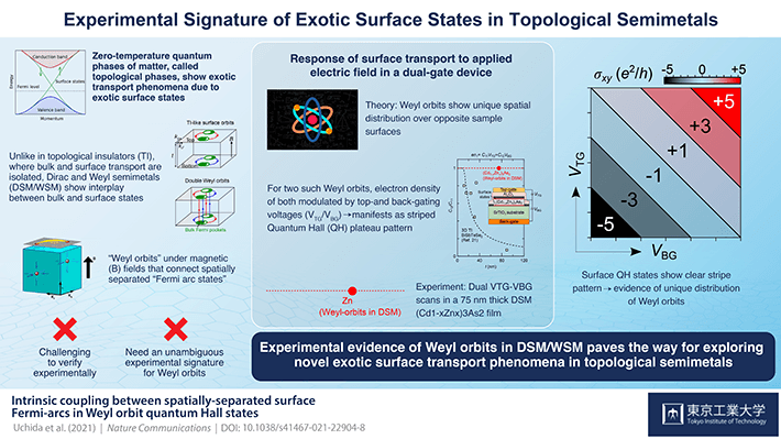
Scientists at Tokyo Institute of Technology experimentally verify the existence of exotic surface conduction states in topological semimetals (TSMs), materials that lie at the boundary between conductors and insulators, by performing voltage scans of these surface states on a thin film sample of a TSM. The findings can pave the way for future study and exploitation of such conduction states in realizing novel, quantum transport phenomena.

All of us are probably familiar with the idea of conductors and insulators. But what would you call a material that can conduct on the surface but insulate on the inside? Physicists call it a "topological insulator" (TI), a term that highlights the geometric aspect of its strange conduction behavior. Even stranger than TIs are "topological semimetals" (TSMs)— bizarre materials that straddle the boundary between metals (conductors) and insulators.
While TIs have found practical applications thanks to their unusual properties, notably in advanced optoelectronic devices, TSMs are still largely a curiosity among material scientists. "In TIs, the surface conduction states can be isolated from the bulk insulating states, whereas in typical TSMs, such as Dirac and Weyl semimetals, the bulk and surface states touch at points called ‘Weyl nodes,’ leading to an interplay between them," explains Associate Professor Masaki Uchida from Tokyo Institute of Technology, Japan, whose research is focused on topological materials.
According to theoretical predictions, an interesting consequence of such an interplay is the formation of a coupled pair of electronic "Weyl orbits" under a magnetic field on opposite surfaces of a TSM that can lead to a novel 2D quantum transport. However, the experimental verification of Weyl orbits has, so far, remained challenging due to the seeming lack of a unique signature. Now, a new study by a team of scientists from Japan, led by Dr. Uchida, might change all that.
Published in Nature Communications, the study focuses on the unique spatial distribution of the Weyl orbits. Specifically, scientists carried out a mapping of Weyl orbit "Quantum Hall" (QH) states under the influence of electric voltages applied on the top and bottom surface of a TSM sample comprising a 75-nm-thick film of (Cd1-xZnx)3As2. "The key observation to distinguish the Weyl orbit from a TI-like orbit is the response of the surface transport to electric fields applied in a dual-gate device configuration," says Dr. Uchida.
Scientists began by studying the magnetic field dependence of film resistance at zero gating voltages at a temperature of 3K (−270°C) and ensured that the film was thick enough to let the Weyl orbits form. Initially, bulk transport dominated the conduction due to a high electron density. However, as scientists depleted the electrons by applying gating voltages, surface transport and its evolution into QH states became more prominent.
Next, the scientists studied the influence of gating voltage scans on these QH states in presence of a strong magnetic field and observed a peculiar striped pattern in the mapped states due to a modulation in their electron density, suggesting the presence of a coupled Weyl orbit pair!
The research team is thrilled by this finding. An excited Dr. Uchida concludes, "Our work revealing the role of unique distribution of Weyl orbits in quantum transport can open doors to finding various exotic surface transport phenomena in TSMs and controlling them via external fields and interface engineering."
The hunt for these novel quantum phenomena is on, with new and exciting discoveries just be around the corner!
Reference
Authors : |
Shinichi Nishihaya1, Masaki Uchida1,2,3, Yusuke Nakazawa1, Markus Kriener4, Yasujiro Taguchi4 and Masashi Kawasaki1,4 |
Title of original paper : |
Intrinsic coupling between spatially-separated surface Fermi-arcs in Weyl orbit quantum Hall states |
Journal : |
Nature Communications |
DOI : |
|
Affiliations : |
1 Department of Applied Physics and Quantum-Phase Electronics Center (QPEC), the University of Tokyo
2 Precursory Research for Embryonic Science and Technology (PRESTO), Japan Science and Technology Agency (JST)
3 Department of Physics, Tokyo Institute of Technology
4 RIKEN Center for Emergent Matter Science (CEMS)
|
. Any information published on this site will be valid in relation to Science Tokyo.


