Main Point
-
Developed chiplet integration technology with excellent broadband chip-to-chip communication and scalable integration
-
Developed chiplet integration technology with novel silicon bridge architecture that uses fine "MicroPillar" and a manufacturing process called "All Chip-last"
-
Highly versatile chiplet integration technology will accelerate the evolution of future semiconductor integrated circuit system technology instead of miniaturization, which is predicted to slow down.
Overview
A research team consisting of Specially Appointed Professor Yoichiro Kurita (Laboratory for Future Interdisciplinary Research of Science and Technology, Institute of Innovative Research, Tokyo Institute of Technology (Tokyo Tech) and a collaborative research company have developed chiplet integration technology[1] that uses a technology called "Pillar-Suspended Bridge (PSB)." This technology meets the requirements for broadband chip-to-chip communication and scalable chiplet integration, which is required for future large-scale chiplet integration, with a minimal configuration and manufacturing process.
It features a silicon bridge interconnection structure via a fine "MicroPillar" for broadband communication between chips and a manufacturing process called "All Chip-last." The structure and the process provide the requirements for chiplet integration in the simplest form. This technology is expected to accelerate the evolution of future semiconductor integrated circuit system technology, replacing miniaturization, which is predicted to slow down.
This research was conducted jointly with Aoi Electronics Co., Ltd. and four other companies ahead of the Chiplet Integration Platform Consortium (described later) to be established on October 1. Detailed results will be presented at the international conference IMAPS 2022, which will be held in Boston, USA, starting October 3 (Monday) at 10 p.m. (Japan time).
In addition to Tokyo Tech, the Chiplet Integration Platform Consortium is centered on Osaka University (Specially Appointed Professor and Professor Emeritus Katsuaki Suganuma) and Tohoku University (Associate Professor Takafumi Fukushima), and 32 companies are scheduled to participate (as of September 2022). It covers research on chiplet integration platform technology in general, including 3D integration technology and optical integration technology.
Background
Since their invention in the middle of the 20th century, semiconductor integrated circuits have become the driving force behind the world's digital transformation thanks to Moore's Law, which improves performance, reduces power consumption, and lowers costs through device miniaturization and improved integration. However, in recent years, the size of semiconductor circuits has been miniaturized to several nanometers. Due to the physical limitations imposed by the size of the atoms that make up a semiconductor, industry now recognizes the law's demise.
Meanwhile, chiplet integration technology (Fig. 1) is in the spotlight as a new evolutionary path to scale up integration and improve performance/reduce power consumption in place of miniaturization. This consists of assembling major systems from a collection of integrated circuit chips that are more tightly coupled than in conventional semiconductor packaging technology. This goes beyond the physical/manufacturing technology dimensions of semiconductor wafers and chips and integrates different functions and structures on a large scale. This makes it possible to provide improved performance through heterogeneous integration and integration scalability, which were not achieved with conventional semiconductor integrated circuit technology.
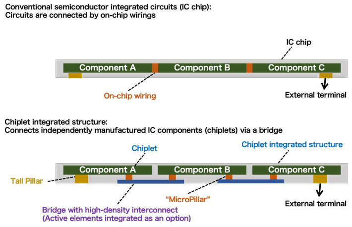
Figure 1. Comparison between conventional semiconductor integrated circuits and chiplet integrated structures
Integration technology using silicon interposers and polymer-based RDL (Redistribution Layer) interposers (also known as RDL-first/Chip-last Fan-Out) has been developed and implemented as a platform technology for chiplet integration, but large-scale integration is limited by wafer size and manufacturing technology. Meanwhile, a technology using locally arranged high-density wiring chips called a silicon bridge is being developed for large-scale integration. However, the complexity of the structure and manufacturing process and the high manufacturing precision required for increased integration present a challenge.
Research results
In view of the above background and challenges, we devised Pillar-Suspended Bridge (PSB) technology as a chiplet integrated structure/process with simplest scheme, and made a proof-of-concept prototype to prove its feasibility. Figures 1 and 2 show a PSB bridge connection structure. Only a pillar-shaped metal called a "MicroPillar" is interposed at the connection between the chiplet and the silicon bridge. The chiplets are sealed with mold resin together with the bridge, and is connected to an external electrode by a "Tall Pillar" penetrating the mold on the silicon bridge side. This structure makes it possible to improve the inter-chip connection density and electrical properties by minimizing the chiplet/bridge interconnect element, and to improve the high-frequency properties of the external connection wiring and heat dissipation performance. Another advantage it has is that the type of bridge wiring can be selected, there is no yield problem when scaling up integration (Known Good Bridge), and the size and manufacturing units of the integrated module can be expanded to large panels. This structure was created by (1) high bonding accuracy and reducing "die shift" (phenomenon in which the chip moves during mold sealing) during the manufacturing process with the All Chip-last process, and (2) a bonding process with matching linear expansion (Coefficient of Thermal Expansion: CTE).
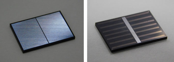
Figure 2. Appearance of proof-of-concept sample of PSB chiplet integrated structure
The PSB structure thus has a simple and rational structure for chiplet integration using silicon bridge. By connecting a wiring layer (e.g., RDL Interposer) with a Fan-Out function to this, it is possible to assemble an ideal chiplet integrated package as shown in Figure 3 or a large-scale chiplet integrated system as shown in Figure 4.
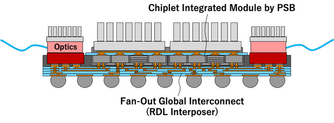
Figure 3. PSB module external connection structure
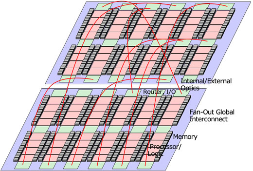
Figure 4. Image of large-scale chiplet integration
Social impact
While the miniaturization of semiconductor integrated circuits is expected to slow down due to Moore's law, chiplet integration technology will likely be a new evolutionary path for improving system performance. This platform technology is expected to have a large effect on human society in the long term, and the emergence of a huge industry accompanying it. This technology and its component technologies and applications are expected to contribute to these trends.
Future development
We plan to increase interconnection density and scale up integration, develop high-performance bridge wiring technology and global wiring integration technology, verify reliability, and verify system applications.
In addition, we will establish the Chiplet Integration Platform Consortium on October 1, 2022 for the purpose of research and development in the value chain from manufacturing technology and element technology to applications and its industrialization, targeting chiplet integration platform technology in general, including this research. Along with Tokyo Tech, the main consortium members are Osaka University (Specially Appointed Professor and Professor Emeritus Katsuaki Suganuma) and Tohoku University (Associate Professor Takafumi Fukushima), and 32 companies are scheduled to participate (as of September 2022). It covers research on chiplet integration platform technology in general, including 3D integration technology and optical integration technology.
Terms
[1]
Chiplet integration technology : Moore's law predicts that the number of components per integrated circuit (chip) will increase exponentially due to transistor miniaturization. From a meta-viewpoint, chiplet integration technology replaces and complements miniaturization in the form of integration of a large number of chips (small chips) to achieve the effect of Moore's law: improved system performance.
Presentation information
Academic conference : |
IMAPS 2022 |
Paper title : |
Chiplet Integration by Die-to-Die Pillar-Suspended Bridge |
Authors : |
Ichiro Kono, Shinji Wakisaka, Toshiaki Hirota, Takashi Saitou, Ken Ukawa, and Yoichiro Kurita |