Main Point
-
Tokyo Institute of Technology (Tokyo Tech) WOW Alliance and the National Cheng Kung University (hereinafter, NCKU) agree on a technical partnership to promote the social implementation (practical application) of next-generation 3D integrated technology based on BBCube.
-
NCKU joins Tokyo Tech WOW Alliance to promote research and development of next-generation 3D technology. A pilot manufacturing line will be established and operated at NCKU, in addition to human resource development.
-
NCKU concludes BBCube business alliance with TECH EXTENSION Co., Ltd. (hereinafter, TEX. Established by Tokyo Tech Specially Appointed Professor Takayuki Ohba). TEX will transfer to NCKU the WOW and COW technologies, which are based on the BBCube platform.
-
Strengthening the semiconductor supply chain through the Tokyo Tech WOW Alliance and Japan-Taiwan BBCube business alliance. A huge leap forward for the social implementation of post-miniaturization next-generation 3D integrated technology.
Overview
The Tokyo Institute of Technology WOW Alliance[1] and NCKU[2] have agreed on a technical partnership for social implementation of Next-generation 3D integrated technology[3] based on BBCube (Bumpless Build Cube)[4]. This is the first Japan-Taiwanese academia alliance for next-generation 3D integration processes. Plans to achieve commercialization will proceed through the BBCube business alliance. NCKU has joined the Tokyo Tech WOW Alliance to participate in research and development of next-generation 3D technology. This includes the construction and testing of a BBCube pilot manufacturing line within the university, as well as developing the necessary human resources for its operation.
A BBCube business alliance was concluded with TEX, a company established by Professor Takayuki Ohba of Tokyo Tech, Institute of Innovative Research. TEX will provide the transfer of WOW Technology[5], and COW Technology[6], both based on the BBCube platform, to NCKU. Processes, equipment, and materials will be utilized, based on the research achievements of the Tokyo Tech WOW Alliance.
Currently, many universities and affiliated companies are participating in the Tokyo Tech WOW Alliance, and are conducting research and development of next-generation semiconductor 3D technology. As industry is entering an age when production yields of cutting-edge semiconductor devices become saturated, due to the increase in invisible defects at the atomic scale, COW chiplet integration and WOW wafer stacking technology becomes ever more important. This Japan-Taiwan collaboration has been formed in response to this need, making product and market orientation seamless, It is expected to promote basic development of post-miniaturization 3D integrated technology and social implementation, as well as strengthening the semiconductor supply chain. The plan is to establish a pilot manufacturing line for R&D at NCKU by the end of 2023, and sequentially apply WOW and COW production processes as BBCube platform technologies.
Scheme : WOW Alliance and BBCube business alliance
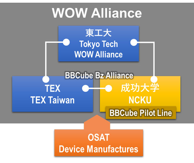
Figure 1. WOW Alliance and BBCube Business Alliance
The Tokyo Tech WOW Alliance, whose aim is to help implement research achievements into society (practical application), established TEX as a Tokyo Tech startup company in 2018. TEX has now concluded a business agreement with NCKU's Innovation Headquarters to establish a BBCube business alliance at NCKU (Figure 1). Research achievements, resulting from the Tokyo Tech WOW Alliance, will be provided through its affiliated company, TEX Taiwan.
OSAT (Out-sourced Semiconductor Assembly and Test), device manufacturers, and other companies are planning to participate in the BBCube business alliance, which is expected to further accelerate social implementation.
A trial manufacturing line for WOW/COW technologies, based on BBCube architecture, will be built at NCKU, and R&D will be conducted with actual equipment, starting from the end of 2022 (phase 1). An integrated line will be established in FY2024 (phase 2). Since it will be possible to simultaneously integrate chiplets at the wafer scale, this integrated line will allow for seamless verification at both the front and back ends.
Technical Overview: Next-generation 3D technology BBCube
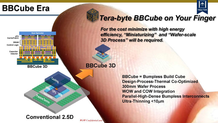
Figure 2. BBCube architecture allowing for system miniaturization
BBCube, developed by the WOW Alliance, makes it possible to minimize the wiring for all constituent devices (memory, CPU, capacitors, etc.) (Figure 2). For example, the distance between capacitors and devices can be reduced from the millimeter to micron level. The WOW Alliance is cooperating on design, process, equipment, and material development, including thermal design, with the aim of miniaturizing beyond "thumb size."
Power consumption with HBM[7], which is used in high-end devices such as servers, is about one-fifth of conventional DDR5[8]. For 2.5D and 3D using BBCube, when the transfer bandwidth reaches the terabyte per second level, the transfer energy per bit is one order of magnitude smaller than with HBM, and the system energy consumption is the world's lowest (less than 10 W) (Figure 3).
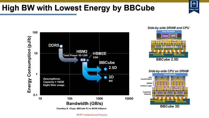
Figure 3. Relationship between power consumption per bit transmission and bandwidth
Up to now, wiring connection requires a protruding bump electrode, formed by plating on the electrode. The resistance of the bump and its high density are an obstacle to speeding up and stacking.
Bumpless technologies such as BBCube are able to avoid such issues. The WOW Alliance has developed technology for thinning wafers to the micron level, and technology for stacking multiple wafers via direct vertical interconnects using TSV[9] (Figure 4). Applying these technologies to DRAM, large memory capacity can be achieved by increasing the number of stacked wafers. This is especially applicable to AI, which requires a large amounts of memory. Under this alliance, bumpless COW has also been developed that makes it possible to have minimum wiring between chips and wafers, allowing for chiplet integration by combining different devices.
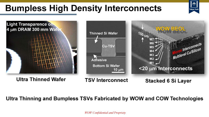
Figure 4. Wafer thinning technology and vertical interconnect technology using TSV
Bumpless interconnects in the BBCube system is a technology that minimizes the vertical connections between chips. Since there are no bumps, the resistance and electrical capacitance are small, and when combined with wafer thinning technology (Si thickness < 4 microns), the TSV wiring length can be the same as the wafer thickness, which improves the electrical properties. Since there are no bump restrictions, the wiring density of TSVs can be increased along with the advancement of lithography, minimizing the space required for TSV on the chip, which had been an issue in the past. This allows better distribution of the TSV inside the chip, and simultaneously minimizing the wiring between chips.
In the case of DRAM chips, if the memory is divided inside the chip and then wired vertically in parallel, typically long-distance signals and power can be transferred in parallel over a short distance instead, via vertical interconnects, proportional to the number of divisions, something that traditionally had to be done on the surface of the chip. This parallelism allows lower power consumption, while maintaining the same transmission bandwidth at lower transmission speeds.
Another advantage of high-density bumpless TSV is better heat dispersion. Conventionally, long TSV wiring and bumps raise the temperature inside the chip as it is stacked, due to long TSV wiring and bumps. The BBC technology greatly relaxes this limit on stacking.
Future Plans
-
From the end of 2022 to the beginning of 2024: Cleanroom establishment and equipment selection (Phase 1)
-
Within FY2024: Trial integrated manufacturing line establishment for research and development (Phase 2)
-
From FY 2025: Mass production according to wafer input
-
Japan-Taiwan semiconductor related industries: Provision of main BBCube technology through trial manufacturing lines
Terms
[1]
WOW Alliance : This is an industry-academia research platform operated by the Heterogeneous and Functional Integration Unit (Ohba Laboratory) of the Institute of Innovative Research, Tokyo Tech. It consists of companies and research institutes that handle design, processing, equipment, and materials related to semiconductors. As the only R&D platform in Japan focused on 3D integration of semiconductors, it pioneered simple wafer thinning and stacking technology with 300 mm wafers. It is also the first in the world to successfully develop 3D technology with bumpless TSV[9] wiring.
[2]
National Cheng Kung University (NCKU) : This is a national university established in 1931. It is well known as a top university in the mid-south region of Taiwan, and is one of six designated national research universities. Official name: 國立成功大學. Tokyo Tech and NCKU entered into an Academic Cooperation Agreement in November 1997.
[3]
Next-generation 3D integrated technology : Next-generation semiconductor technology with 3D integration at the wafer level. Based on the ultra-thinning technology and bumpless vertical wiring technology owned by the WOW Alliance, it is possible to achieve 3D integration with semiconductors that allows for higher performance and lower power consumption than with conventional products. In addition to large-scale computing devices such as servers, the size of mounted multifunction device systems can be greatly reduced.
[4]
BBCube (Bumpless Build Cube) : Architecture allowing systems to be minimized without the use of bumps. It is a compact 3D version of a chiplet, which are conventionally a flat plane.
Reference: Ohba, T.; Sakui, K.; Sugatani, S.; Ryoson, H.; Chujo, N. Review of Bumpless Build Cube (BBCube) Using Wafer-on-Wafer (WOW) and Chip-on-Wafer (COW) for Tera-Scale Three-Dimensional Integration (3DI). Electronics 2022, 11, 236. DOI: 10.3390/electronics11020236
[5]
WOW (Wafer-on-Wafer) Technology : Stacking technology that allows wafers to be directly bonded and connected to each other. This greatly helps to improve efficiency of wafer stacking of the same chip size such as for DRAM.
[6]
COW (Chip-on-Wafer) Technology : Technology that connects and bonds chiplets on a wafer using WOW technology. By bonding the chips directly onto the wafer, high-precision processing can be performed using various types of wafer processing equipment in subsequent semiconductor manufacturing processes.
[7]
HBM (High Bandwidth Memory) : A memory standard by JEDEC that assumes die stacking using Through Silicon Via (TSV)[9]) technology.
[8]
DDR5 SDRAM (Double Data Rate 5 Synchronous Dynamic Random-Access Memory) : A type of DRAM standard composed of semiconductor integrated circuits. It is used as the main memory of a computer, as a memory module (DIMM = Dual Inline Memory Module), where multiple DRAM chips are mounted to a printed board. Compared to the previous generation of DDR4 SDRAM, DDR5 has double the bandwidth, while consuming less power.
[9]
TSV (Through-Silicon-Via) : A connection hole (Via) opened through the silicon wafer. The vertically stacked chips are connected by embedded wiring. Since wiring is recently being done for materials other than silicon, it can be also referred to as a vertical interconnect during front-end processing.