Ultra-Thinning of 300-mm Wafer Down to 4-micrometer Thickness
Ultra-Thinning of 300-mm Wafer Down to 4-µm Thickness
-Proven by DRAM, applicable for the next Three Dimensional Large Scale Memories-
Summary
Professor Takayuki Ohba, the Tokyo Institute of Technology, ICE Cube Center, in collaboration with DISCO Corporation, Fujitsu Laboratories Ltd., PEZY Computing (Chiyoda-ku, Tokyo), and the WOW Alliance (1), has developed technology for the ultra-thinning process down to 4 micrometer (µm) using 300mm wafer implemented 2G bit DRAM memory. The ultra-thinning process was carried out by the bumpless WOW 3D process (2) consist of no bumps TSV (3) and succeeded the thickness of the 300mm silicon wafers down to 4µm, thinner than the device layer, for the first time.
It was confirmed that there were no changes in the probability failure rate of refresh times before and after thinning-down, which means no new atomic defects occurred due to the thinning process. Using these thinned wafers, the length of the wiring between upper- and lower-layer chips is reduced to below 1/10 compared to conventional TSVs, with wiring resistance, capacitance, and volume being reduced drastically. It is expected to realize applications in ultra-small, Terabit (1 Tera is 1,000,000,000,000)-generation large-scale memory.
The results of this research were reported at the International Electron Device Meeting “VLSI Symposium 2014” held in Hawaii on June 10-13.
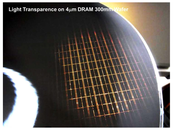
A 300mm DRAM wafer thinned-down to 4µm. When wafers become this thin visible light permeates them.
Explanation of Technical Terms
1. WOW Alliance: |
A research group conducting at the Tokyo Institute of Technology and cooperated with semiconductor-related companies including design, process, device, materials, and research institutions. It succeeded in the world's first development of the bumpless TSV 3D technology, enabling wafer stack easily even thinned-down wafers. |
2. WOW 3D technology: |
3D integration technology for making large-scale integrated circuits by wafer stack (Wafer-on-Wafer). There is stack methods including Chip-on-Chip (COC) and Chip-on-Wafer (COW) and productivity increased in the order of COC < COW < WOW. |
3. Bumps: |
Joint metal material formed by electroplating method. |
Reference
Presenter: |
Y.S. Kim, S. Kodama, Y. Mizushima, N. Maeda, H. Kitada, K. Fujimoto, T. Nakamura, D. Suzuki, A. Kawai, K. Arai and T. Ohba |
Title of presentation: |
Ultra Thinning Down to 4-µm using 300-mm Wafer40-nm Node 2Gb DRAM for 3D Multi-Stack WOW Applications |
Conference: |
IEEE 2014 Symposia on VLSI Technology and Circuits |