Researchers use simulations to identify previously undiscovered semiconductors with promising attributes for optical and electronic applications. A nitride among those proposed has been successfully fabricated using high-pressure synthesis and is found to emit red light.
The discovery of new semiconducting materials is a scientifically and technologically important issue; state researchers in Japan in a recent report. Increasingly sophisticated electronic devices, such as smartphones and laptops, are raising demand for semiconductors with wider ranges of properties. Now Fumiyasu Oba and colleagues at Tokyo Institute of Technology and Kyoto University have used calculations to screen a set of compounds for potential semiconductor candidates. The study identified 11 previously unreported materials, including the particularly promising compound calcium zinc nitride (CaZn2N2).
The researchers limit their study to nitrides because they tend to be chemically stable and can be readily made with existing techniques. Nitrogen is also a widely abundant and environmentally friendly element, but, at present, the nitrides used in industry are largely limited to gallium and indium compounds. Based on similarities in the electronic structure, the researchers rationalised that ternary zinc nitrides would be promising compounds to consider for new semiconductors in this field.
The researchers highlight the previously unreported semiconductor CaZn2N2, which should have a high electrical conductivity and a strong interaction with light. These properties are indicators of good performance in optoelectronic applications such as light emitting diodes (LEDs) and solar cells. It is also made entirely of earth-abundant elements and so can be relatively cheap to make.
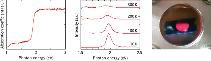
Synthesis of the material using high-pressure techniques confirmed the hypothesised properties and also revealed red luminescence even at room temperature; thereby validating the study's approach. The paper also shows that other earth-abundant materials, such as calcium magnesium nitride, can be used to tune the electrical properties of CaZn2N2, further increasing the eligibility of this material for use in devices.
As Oba and colleagues conclude, "The present study demonstrates accelerated materials discovery via cutting-edge computational screening followed by targeted experiments."
Background
Limitations of existing semiconductors
Silicon and, to a lesser degree, germanium are the foundations of almost all electronic devices that govern modern life. However, these materials are not suited for optoelectronic applications, such as LEDs for TV or mobile phone screens. Here, the materials gallium nitride (GaN) and indium nitride (InN) dominate currently, but the discovery of new nitrides could pave the way to new applications.
Foremost among the characteristics Oba and colleagues sought in any new compound was high conductivity, which is crucial for most semiconductor applications. GaN and InN have spatially diffuse orbital characteristics, which result in the high electrical conductivity that has led to their success. The researchers considered materials with such properties similar to GaN and InN in order to find new industry-relevant semiconductors. Zinc nitride has these desirable properties but is difficult to make. As a result, the researchers decided to screen for ternary compounds comprising zinc, nitrogen and a third element. This approach led to the identification of 11 new materials, including the exciting CaZn2N2.
Earth abundant elements
Rare elements can confer many useful properties in semiconductor compounds but they are increasingly difficult to extract and their processing costs can be very expensive. As a result, there is an increasing interest in earth-abundant materials that may be used as alternatives. By using nitrogen and zinc components as criteria for their screening methods, Oba and colleagues are able to maximize the chances of cost competitiveness for their discoveries compared to known materials.
Calcium zinc nitride
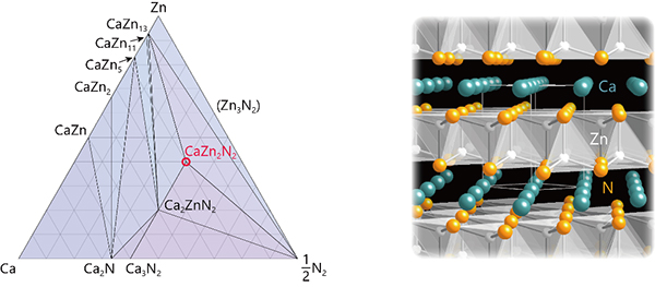
CaZn2N2 has not been reported previously but was identified by the researchers using their materials discovery computational approach. They were also able to predict the correct synthesis conditions for CaZn2N2, leading to the successful formation of the new compound using high-pressure synthesis. Further experiments confirmed that the compound has a direct bandgap and favourable optical properties.
Figure 1. Predictions on the stability and crystal structure of CaZn2N2. Left: Ca–Zn–N ternary phase diagram. Right: Crystal structure of CaZn2N2. Only the Zn–N bonds are illustrated for easy visualization.
Figure 2. Optical properties of CaZn2N2. Left: Photoabsorption spectrum. Middle: Photoluminescence spectra at temperatures of 10, 100, 200, and 300 K. Right: Photograph of red photoluminescence at 10 K.
Reference
Authors: |
Yoyo Hinuma1,2, Taisuke Hatakeyama3, Yu Kumagai4, Lee A. Burton3, Hikaru Sato3, Yoshinori Muraba4, Soshi Iimura3, Hidenori Hiramatsu3,4*, Isao Tanaka1,2, Hideo Hosono3,4, Fumiyasu Oba1,2,3,4 * |
Title of original paper: |
Discovery of earth-abundant nitride semiconductors by computational screening and high-pressure synthesis |
Journal: |
Nature Communications |
DOI: |
|
Affiliations: |
1Department of Materials Science and Engineering, Kyoto University
2Center for Materials Research by Information Integration, National Institute for Materials Science
3Laboratory for Materials and Structures, Institute of Innovative Research, Tokyo Institute of Technology
4Materials Research Center for Element Strategy, Tokyo Institute of Technology
*Corresponding authors |