Scientists at Tokyo Tech have successfully developed n-type semiconducting copolymers with high electron mobilities. They investigated their properties and their effectiveness for thin-film transistors, obtaining highly promising results.
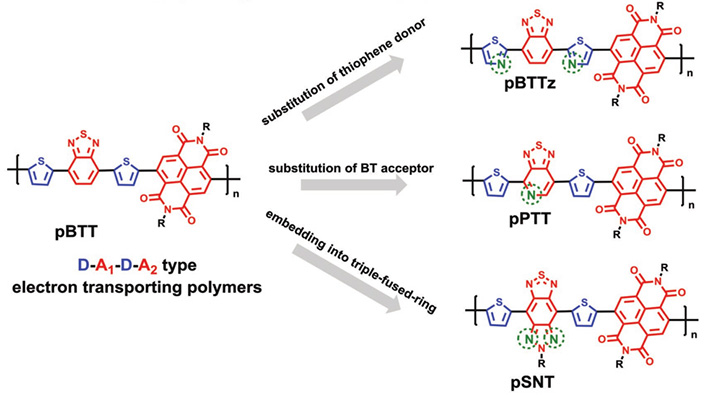
Figure 1. Design of the three n-type semiconducting polymers.
By strategic embedding of sp2-N atoms in BTT, three different polymers were synthesized and used to fabricate thin-film transistors.
Semiconducting polymers have numerous potential applications in modern technological devices owing to their low cost, low weight, and flexibility. In particular, this type of polymers has emerged as an exciting variant as they can be used to create thin-film transistors (TFTs), which can be used as the building blocks for the circuitry of rollable displays, nonvolatile memory, electronic skin, sensors, and many other printed electronic devices.
In recent years, there has been enormous progress in p-type (hole-transporting) semiconducting polymers. Yet, reports on high-mobility n-type (electron-transporting) semiconducting polymers are rare. Motivated by the potential applications of n-type semiconducting polymers, such as in CMOS-like logic circuits, organic thermoelectric devices, and solar cells, scientists at the Tokyo Tech, led by Associate Professor Tsuyoshi Michinobu and Dr Yang Wang, decided to address the fundamental challenges in this field.
They devised a reliable method for synthesizing three different n-type semiconducting polymers with a high molecular weight, which, if optimized, has a positive effect on electron mobilities. They tested the properties of the synthesized polymers, which are based on benzobisthiadiazole (BBT) derivatives, when used in TFTs. Their aim was to find a way to lower the transistors' threshold voltages and off-current values, which would otherwise severely limit their potential fields of application.
The protocol for the polymerization process that the researchers designed is based on the Stille reaction, which has been widely used in organic chemistry since the 1970s. However, they used a modified version of this process with optimized catalysts, solvents, and reactant ratios, to consistently obtain high-molecular-weight polymers. Three different types of polymers were designed by embedding nitrogen atoms in strategic locations of the BBT molecules, and TFTs were made using each type of polymer to compare their performances.
To further improve the performance of their TFTs, the team decided to use an amine-based self-assembled monolayer (SAM) to cover the SiO2 layer. SAMs have been known to improve carrier mobility in p-type semiconducting polymers and provide a way to control surface roughness. However, traditional SAMs are made of octadecylsilanes, which would degrade the performance of the proposed n-type semiconducting-polymer-based TFTs. Using a simple spin coating process, the researchers were able to form a smooth amine SAM for the TFTs.
Once built, the TFTs were thoroughly analyzed via various measurements to check their surface properties, electrical characteristics, crystallinity, and overall structure. After testing, the researchers found out the differences in the TFT properties resulting from the use of their three different semiconducting polymers. An unprecedented unipolar electron mobility of 5.35 cm2 V-1 s-1 was obtained with their best-performing polymer, along with very small threshold voltage and off-current values. The researchers have stated that further research will be carried out in order to further exploit their n-type semiconducting polymers so that they find their way into modern applications.
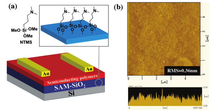
Figure 2. Layers of the thin-film transistors.
(a) Structure of the thin-film transistors with the proposed SAM layer and polymers. (b) Atomic force microscopy image of the SAM layer, demonstrating its smoothness.
Reference
Authors : |
Yang Wang, Tsukasa Hasegawa, Hidetoshi Matsumoto, Takehiko Mori, and Tsuyoshi Michinobu |
Title of original paper : |
High-Performance n-Channel Organic Transistors Using High-Molecular-Weight Electron-Deficient Copolymers and Amine-Tailed Self-Assembled Monolayers |
Journal : |
Advanced Materials |
DOI : |
|
Affiliations : |
Tokyo Institute of Technology
|