Each issue of the journal Nature Electronics contains a column called "Reverse Engineering," which examines the development of an electronic device now in widespread use from the viewpoint of the main inventor. So far, it has featured creations such as the DRAM, DVD, CD, and Li-ion rechargeable battery. The July 2018 column tells the story of the IGZO thin film transistor (TFT) through the eyes of Professor Hideo Hosono of Tokyo Tech's Institute of Innovative Research (IIR), who is also director of the Materials Research Center for Element Strategy.

TFTs using oxides including indium (In), gallium (Ga), and zinc (Zn), or IGZO, made possible high-resolution energy-efficient displays that had not been seen before. IGZO electron mobility is 10 times that of hydrogenated amorphous silicon, which was used exclusively for displays in the past. Additionally, its off current is extremely low and it is transparent, allowing light to pass through. IGZO has been applied to drive liquid crystal displays, such as those on smartphones and tablets. Three years ago, it was also used to drive large OLED televisions, which was considered a major breakthrough. This market is rapidly expanding, as can be seen from the products being released by South Korean and Japanese electronics manufacturers, which now dominate store shelves.
The electron conductivity of transition metal oxides has long been known, but electric current modulation using electric fields has not. In the 1960s, it was reported that modulating the electric current was possible when zinc oxide, tin oxide, and indium oxide were formed into TFT structures. Their performance, however, was poor, and reports of research on organic TFTs were mostly nonexistent until around 2000. A new field called oxide electronics came into existence in the early noughties, examining oxides as electronic materials. A hub for this research was the present-day Laboratory for Materials and Structures within IIR, and research into zinc oxide TFTs soon spread worldwide. However, since the thin film was polycrystalline, there were problems with its characteristics and stability, and no practical applications were achieved.
Application in displays, unlike CPUs, requires the ability to form a thin, homogenous film on a large-sizedsubstrate — like amorphous materials — and a dramatic increase in electric current at a low gate voltage when the thin film is subjected to an electric field. However, while amorphous materials were the optimal choice for forming thin, homogeneous film, high carrier concentration and other issues due to structural disorder arose, for the most part preventing electric current modulation by electric fields. The only exception was amorphous silicon containing a large amount of hydrogen, reported in 1975. TFTs made of this material were applied to drive liquid crystal displays, which grew into a giant 10 trillion-yen industry. However, electron mobility was still lower by two to three orders of magnitude compared to that of crystalline silicon — no better than 0.5 to 1 cm2 V-1 s-1. Amorphous semiconductors, therefore, were easy to produce, but were seen to have much inferior electronic properties.
Hosono focused his attention on oxides with highly ionic bonding nature, the series made up of non-transition metals belonging to the p-block of the periodic table. In this material series, the bottom of the conduction band, which works as the path for electron, is made up mainly of spherically symmetrical metal s-orbitals with a large spatial spread. Because of this, the degree of overlap of the orbitals, which govern how easily electrons can move, is not sensitive to bond angle variation which is an intrinsic nature of amorphous materials.
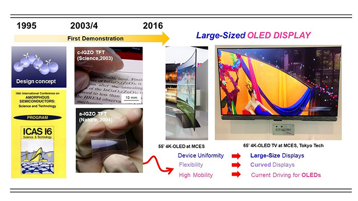
The professor realized that this characteristic might allow for mobility in amorphous materials that is comparable to that of polycrystalline thin films. He experimented accordingly, and was able to find some examples. In 1995, he presented his idea and examples at the 16th International Conference on Amorphous Semiconductors, and had the paper on its proceedings published the following year. After proving this hypothesis through experiments and calculations, he started test-producing TFTs. Many combinations of elements fulfilled the conditions of the hypothesis. IGZO was selected because it had a stable crystalline phase that is easy to prepare, and its specific local structure around Ga suggested that carrier concentration could be suppressed. In 2003, Hosono and his collaborators reported in Science that crystalline epitaxial thin film could produce mobility of around 80 cm2 V-1 s-1. In the following year, they published in Nature that amorphous thin film could also produce mobility of around 10 cm2 V-1 s-1.
Following these findings, research on amorphous oxide semiconductors and their TFTs began increasing rapidly around the world — not just among the Society for Information Display (SID) and the International Conference on Amorphous Semiconductors. This activity has continued, and Hosono's two papers have now been cited over 2,000 and 5,000 times respectively. The total citations of the patents associated with these inventions now exceed 9,000. Products with displays incorporating these TFTs have been available to the general consumers since 2012. In particular, large OLED televisions, which appeared around 2015, became possible only due to the unique characteristics of amorphous IGZO TFTs — their high mobility and ability to easily form a thin, homogenous film over a large area. Such displays are installed on the first floor of the Materials Research Center for Element Strategy and the foyer of the Laboratory for Materials and Structures at Tokyo Tech. Application of IGZO TFTs to high-definition large LCD televisions are expected to start soon.
The outcomes of this research are a result of the Japan Science and Technology Agency (JST) ERATO Transparent ElectroActive Materials project, carried out from 1999 to 2004. Related intellectual property has been established in many countries and regions including Japan, U.S.A., South Korea, mainland China, Taiwan, India, various European countries and so on. The principal patentee, JST, handles the granting of licenses.
Reference
Journal : |
Hideo Hosono, How we made the IGZO transistor, Nature Electronics , vol.1, July issue, 2018 |
DOI : |
|
IGZO TFT-related papers : |
K.Nomura, H.Ohta, K.Ueda, T.Kamiya, M.Hirano, H.Hosono, Thin-film transistor fabricated in single-crystalline transparent oxide semiconductor. Science, 300, 1269 (2003).
K.Nomura, H.Ohta, A.Takagi, T.Kamiya, M.Hirano, H.Hosono, Room-temperature fabrication of transparent flexible thin-film transistors using amorphous oxide semiconductors. Nature, 432, 488 (2004).
|
Reviews : |
H.Hosono, Ionic amorphous oxide semiconductors: Material design, carrier transport, and device application, J.Non-Crystalline Solids, 352 , 851 (2006)
T.Kamiya, H.Hosono, Material characteristics and applications of transparent amorphous oxide semiconductors, NPG Asia Materials, 2, 15 (2010)
|
. Any information published on this site will be valid in relation to Science Tokyo.


