


Tokyo Tech News
Tokyo Tech News
![]()
Published: August 23, 2023
A novel ferroelectric semiconductor memory developed by researchers from Tokyo Tech, dedicated proponents of semiconductor advancements, is an exciting prospect for memory storage technology. It promises to open novel data storage and processing capabilities, paving the way for faster and more energy-efficient devices.
Traditional memory technologies face limitations in terms of speed, scalability, and power consumption, making them unsuitable for future data-intensive applications. Ferroelectric memory has garnered immense interest in recent years due to its potential for non-volatile storage, enabling data retention even when the power is turned off. The development of two-dimensional (2D) van der Waals material α-In2Se3 has also opened new opportunities for advancing memory technologies.
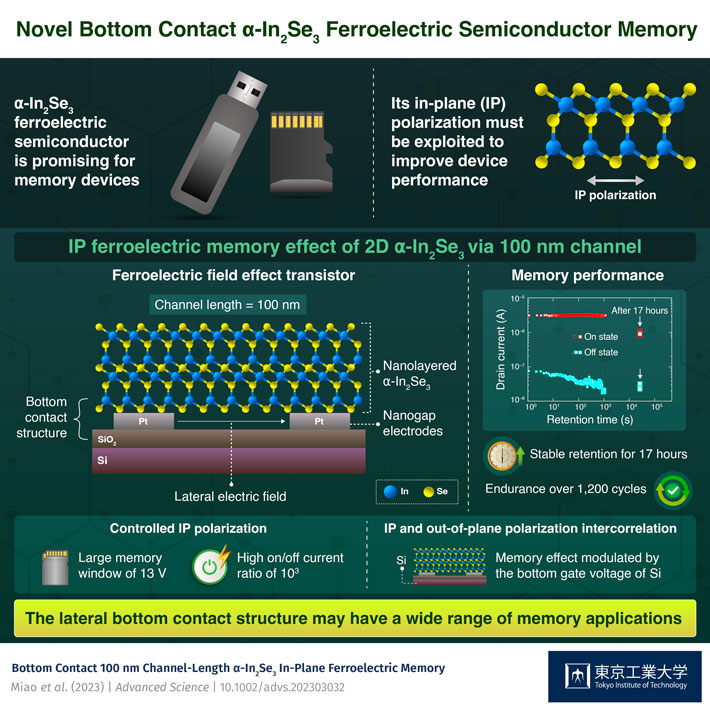
Interestingly, ferroelectric memory takes a giant step forward by incorporating the remarkable properties of α-In2Se3. It is renowned for high carrier mobility, tunable bandgap, and strong ferroelectric properties at the atomic level, making it ideal for high-speed memory applications. However, the scope of research is limited by the lack of lateral α-In2Se3 devices that demonstrate in-plane (IP) polarization-controlled electrical characteristics. When fabricating bottom-contact ferroelectric field-effect transistors by 2D material exfoliation, wide electrode width is preferred to improve the overall yield. However, achieving nanoscale channel lengths for the nanogap electrodes becomes challenging when simultaneously employing wide electrode widths, mainly due to the substantial ratio between the electrode width and channel length.
Recently, a team of researchers led by Professor Yutaka Majima from Tokyo Institute of Technology (Tokyo Tech) proposed a new concept of bottom contact structure at the nano level to solve this problem. They have designed a ferroelectric semiconductor memory device with a two-terminal nanogap-structured bottom contact by leveraging the IP polarization flipping of α-In2Se3. Their work is published in Advanced Science.
Distinct from previous devices, α-In2Se3 is exfoliated on electrodes as the bottom contact in the present design. The IP polarization can be reversed by applying a drain voltage via a channel with a relatively narrow length of 100 nm. This lateral channel design allows for higher memory density, enabling the integration of many memory cells on a single chip. Furthermore, the lateral memory configuration employed in the proposed technology enables seamless integration with existing semiconductor device fabrication techniques, facilitating a smooth transition from current memory technologies to non-volatile ferroelectric memory.
The researchers found that the α-In2Se3 ferroelectric memory exhibits typical resistive switching, a high on/off ratio of over 103, a large memory window of 13 V, good retention for 17 hours, and endurance for 1,200 cycles. This will pave the way for non-volatile ferroelectric memory. Notably, massive integration becomes promising with a bottom contact structure, considering the simplified construction of next-generation electronics.
"Our ferroelectric semiconductor memory cultivates the IP polarization α-In2Se3 from a 100 nm bottom contact design, representing a significant leap forward in memory technology," says Prof. Majima. "We believe that this design will pave the way in which data is stored and accessed and open up exciting opportunities for various applications, including artificial intelligence, edge computing, and Internet of Things devices."
With the unveiling of this cutting-edge ferroelectric semiconductor memory, Prof. Majima reaffirms their commitment to pushing the boundaries of semiconductor technology and driving innovation in this field. Amidst the growing demand for higher performance and energy-efficient memory solutions, their team remains dedicated to delivering advanced and reliable solutions to meet the ever-evolving needs of the digital era.
Reference
Authors : |
Shurong Miao1, Ryosuke Nitta1, Seiichiro Izawa1,2, and Yutaka Majima1,* |
Title : |
Bottom Contact 100 nm Channel-Length α-In2Se3 In-Plane Ferroelectric Memory |
Journal : |
Advanced Science |
DOI : |
|
Affiliations : |
1 Laboratory for Materials and Structures, Institute of Innovative Research, Tokyo Institute of Technology 2 Joining and Welding Research Institute, Osaka University |
* Corresponding author's email: majima@msl.titech.ac.jp
Further Information
Professor Yutaka Majima
Institute of Innovative Research, Tokyo Institute of Technology
Email majima@msl.titech.ac.jp
Contact
Public Relations Division, Tokyo Institute of Technology
Email media@jim.titech.ac.jp
Tel +81-3-5734-2975

![]()
© Tokyo Institute of Technology. All rights reserved.
![]()