New phased-array transmitter design overcomes common problems of CMOS technology in the 300 GHz band, as reported by scientists from Tokyo Tech. Thanks to its remarkable area efficiency, low power consumption, and high data rate, the proposed transmitter could pave the way to many technological applications in the 300 GHz band, including body and cell monitoring, radar, 6G wireless communications, and terahertz sensors.
Today, most frequencies above the 250 GHz mark remain unallocated. Accordingly, many researchers are developing 300 GHz transmitters/receivers to capitalize on the low atmospheric absorption at these frequencies, as well as the potential for extremely high data rates that comes with it.
However, high-frequency electromagnetic waves become weaker at a fast pace when travelling through free space. To combat this problem, transmitters must compensate by achieving a large effective radiated power. While some interesting solutions have been proposed over the past few years, no 300 GHz-band transmitter manufactured via conventional CMOS processes has simultaneously realized high output power and small chip size.
Now, a research team led by Professor Kenichi Okada from Tokyo Institute of Technology (Tokyo Tech) and NTT Corporation (Headquarters: Chiyoda-ku, Tokyo; President & CEO: Akira Shimada; "NTT") have recently developed a 300 GHz-band transmitter that solves these issues through several key innovations. Their work will be presented in the 2024 IEEE International Solid-State Circuits Conference (ISSCC).
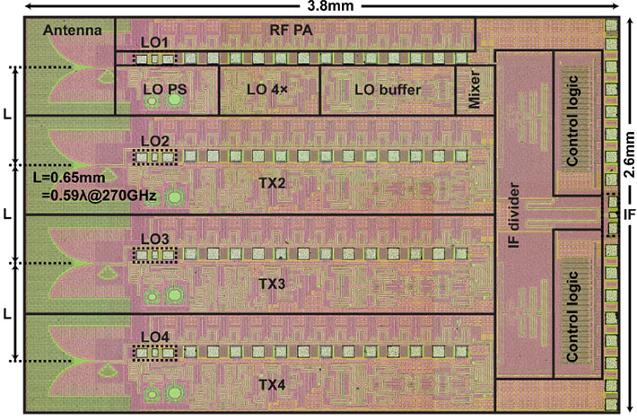
The proposed solution is a phased-array transmitter composed of 64 radiating elements, which are arranged in 16 integrated circuits with four antennas each. Since the elements are arranged in three dimensions by stacking printed circuit boards (PCBs), this transmitter supports 2D beam steering. Simply put, the transmitted power can be aimed both vertically and horizontally, allowing for fast beam steering and tracking receivers efficiently. Notably, the antennas used are Vivaldi antennas, which can be implemented directly on-chip and have a suitable shape and emission profile for high frequencies.

Figure 1. Chip die micrograph
The proposed transmitter chip could pave the way for enhanced body and cell monitoring, radar, 6G wireless communications, and terahertz sensors.

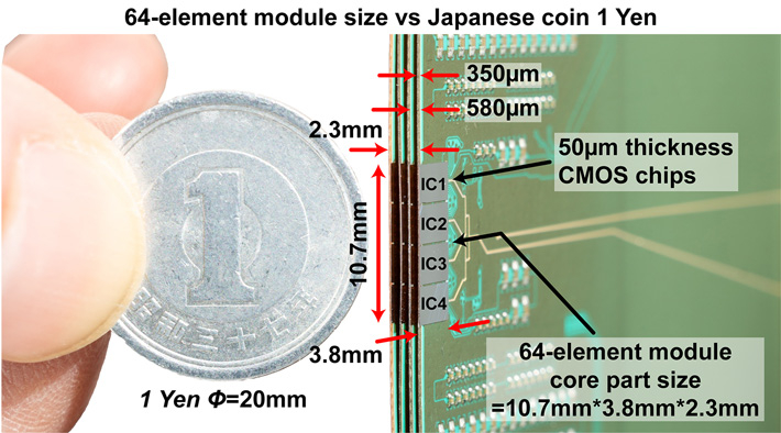
Figure 2. Compact phased-array transmitter with on-chip antennas
Thanks to a highly optimized circuit topology and layout, the proposed transmitter chips can be arranged into a 64-element array occupying a minuscule volume.
An important feature of the proposed transmitter is its power amplifier (PA)-last architecture. By placing the amplification stage right before the antennas, the system only needs to amplify signals that have already been conditioned and processed. This leads to higher efficiency and better amplifier performance.
The researchers also addressed a few common problems that arise with conventional transistor layouts in CMOS processes, namely high gate resistance and large parasitic capacitances. They optimized their layout by adding additional drain paths and vias and by altering the geometry and element placing between metal layers. "Compared to the standard transistor layout, the parasitic resistance and capacitances in the proposed transistor layout are all mitigated," remarks Prof. Okada. "In turn, the transistor-gain corner frequency, which is the point where the transistor's amplification starts to decrease at higher frequencies, was increased from 250 to 300 GHz."
On top of these innovations, the team designed and implemented a multi-stage 300 GHz power amplifier to be used with each antenna. Thanks to excellent impedance matching between stages, the amplifiers demonstrated outstanding performance, as Prof. Okada highlights: "The proposed power amplifiers achieved a gain higher than 20 dB from 237 to 267 GHz, with a sharp cut-off frequency to suppress out-of-band undesired signals." The proposed amplifier also achieves a noise figure of 15 dB which was evaluated by the noise measurement system in 300-GHz band.
The researchers tested their design through both simulations and experiments, obtaining very promising results. Remarkably, the proposed transmitter achieved a data rate of 108 Gb/s in on-PCB probe measurements, which is substantially higher than other state-of-the-art 300 GHz-band transmitters.
Moreover, the transmitter also displayed remarkable area efficiency compared to other CMOS-based designs alongside low power consumption, highlighting its potential for miniaturized and power-constrained applications. Some notable use cases are sixth-generation (6G) wireless communications, high-resolution terahertz sensors, and human body and cell monitoring.
Make sure to stay tuned for future technological developments in the 300 GHz band!
. Any information published on this site will be valid in relation to Science Tokyo.


