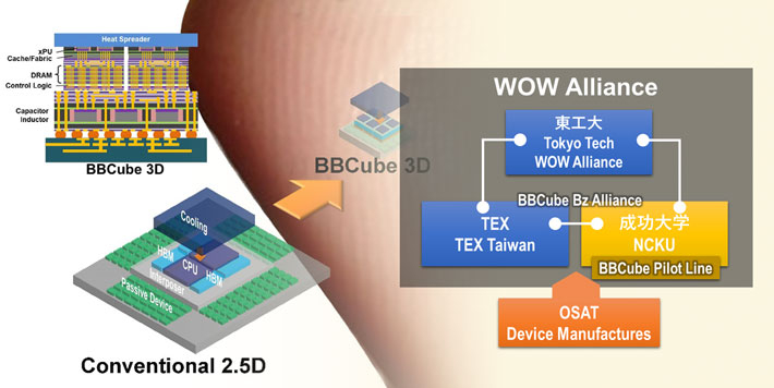
Tokyo Institute of Technology's WOW Alliance[1] has facilitated a groundbreaking agreement between Tech Extension Co., Ltd. (TEX)[2], Tech Extension Taiwan Co., Ltd. (TEX-T)[3], and Innolux Corporation (INNOLUX)[4] to construct a next-generation 3D integration[5] manufacturing line using the Bumpless Build Cube (BBCube)[6] technology in an INNOLUX cleanroom.
TEX will transfer WOW technology[7] and COW technology[8], which are both based on the BBCube technology platform, to this manufacturing line intended for next-generation 3D integration. This technology transfer utilizes processes, equipment, and materials.
Also, TEX and TEX-T will take the lead in building the next-generation 3D integration manufacturing line and are scheduled to concurrently conduct research and development, including human resource development, in collaboration with the Tokyo Tech WOW Alliance, National Cheng Kung University (NCKU)[9], and other universities and industries.
A next-generation semiconductor integrated manufacturing line that encompasses manufacturing from WOW manufacturing to COW manufacturing will be built to take advantage of the WOW and COW technologies, which are based on the platform for BBCube technology possessed by TEX and TEX-T, aiming at utilizing the WOW and COW technologies as post-miniaturization core technologies.
In the future, equipment will be launched sequentially from Q4 in 2024, and an integrated manufacturing line is scheduled to be launched by Q3 in 2025, thus sequentially applying the WOW and COW technologies, which are based on the BBCube platform.
Terms
[1]
WOW Alliance : This is an industry-academia research platform operated by the Heterogeneous and Functional Integration Unit (Ohba Laboratory) of the Institute of Innovative Research, Tokyo Tech. It consists of companies and research institutes that handle design, processing, equipment, and materials related to semiconductors. As the only R&D platform in Japan focused on 3D integration of semiconductors, it pioneered simple wafer thinning and stacking technology with 300 mm wafers. It is also the first in the world to successfully develop 3D technology with bumpless TSV wiring.
[2]
TECH EXTENSION Co., Ltd. : Venture company initiated by Tokyo Institute of Technology established on January 16, 2018 by Professor Takayuki Ohba of Tokyo Institute of Technology, Institute of Innovative Research, with the aim of implementing BBCube technology in society. Headquartered in Tokyo, Japan.
[3]
TECH EXTENSION TAIWAN CO., LTD. : Local affiliated company established by TEX in Taiwan on November 2, 2020, with the aim of conducting full-scale activities in Taiwan. Headquartered in Taipei, Taiwan.
[4]
Innolux Corporation : I Innolux was founded in 2003 and went public in Taiwan in 2006. In March 2010, its merger with Chi Mei Optoelectronics and TPO Displays marked the largest merger in the history of the panel industry. Innolux integrates the product manufacturing supply chain and provides customers with complete solutions through its innovative operation approach of panel-centric and vertical integration. Not only does Innolux have a good TFT-LCD foundation and production quality, but it also has a strong focus on processing technology and components, as well as excellent management capabilities.
[5]
Next-generation 3D integration : This refers to next-generation semiconductor technology with 3D integration at the wafer level. Based on the ultra-thinning technology and bumpless vertical wiring technology owned by the WOW Alliance, it is possible to achieve 3D integration with semiconductors that allows for higher performance and lower power consumption than with conventional products. In addition to large-scale computing devices such as servers, this makes it possible greatly reduce the size of mounted multifunction device systems.
[6]
BBCube (Bumpless Build Cube) : Architecture allowing systems to be minimized without the use of bumps. It is a compact 3D version of a chiplet, which are conventionally a flat plane.
Reference: Ohba, T.; Sakui, K.; Sugatani, S.; Ryoson, H.; Chujo, N. Review of Bumpless Build Cube (BBCube) Using Wafer-on-Wafer (WOW) and Chip-on-Wafer (COW) for Tera-Scale Three-Dimensional Integration (3DI). Electronics 2022, 11, 236. DOI: 10.3390/electronics11020236
[7]
WOW (Wafer-on-Wafer) Technology : Stacking technology that allows wafers to be directly bonded and connected to each other. This greatly helps to improve efficiency of wafer stacking of the same chip size such as for DRAM.
[8]
COW (Chip-on-Wafer) Technology : Technology that connects and bonds chiplets on a wafer using WOW technology. By bonding the chips directly onto the wafer, high-precision processing can be performed using various types of wafer processing equipment in subsequent semiconductor manufacturing processes.
[9]
National Cheng Kung University (NCKU) : This is a national university established in 1931. It is well known as a top university in the mid-south region of Taiwan, and is one of six designated national research universities. Official name: 國立成功大學. Tokyo Tech and NCKU entered into an Academic Cooperation Agreement in November 1997.
. Any information published on this site will be valid in relation to Science Tokyo.


