Advanced electronic devices require high-quality materials such as metal halide phosphors that can effectively convert light into measurable signals. Toxic element-free copper-based iodides such as cesium copper iodide (Cs3Cu2I5: CCI) are particularly promising in this regard. CCI is an efficient blue light-emitting material that can convert almost all the absorbed energy into detectable light, making them ideal for use in deep-UV photodetectors and γ-ray scintillators for detecting ionizing radiation, such as gamma or X-rays. However, the thin films of CCI do not meet the required quality standards, hindering their performance improvement for advanced stacking applications.
Now, a study published in the Journal of the American Chemical Society has addressed this issue by proposing an innovative method for producing high-quality thin films of Cs3Cu2I5. The study was led by researchers from Tokyo Institute of Technology (Tokyo Tech), including Professor Hideo Hosono as the corresponding author and Specially Appointed Assistant Professor Masatake Tsuji as the first author.
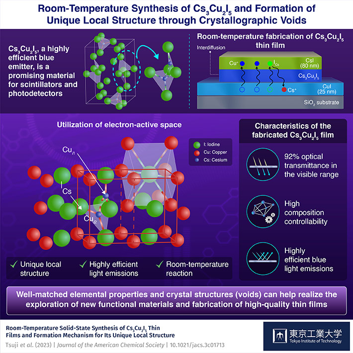
In an earlier experimental finding, the team had discovered that cesium iodide (CsI) and copper iodide (CuI) powders can react even at room temperature to form Cs3Cu2I5. Building on this insight, they deposited thin films of CuI and CsI onto a silica substrate by evaporating them in a vacuum chamber. The two films were then allowed to react at room temperature to form transparent and highly smooth films with a high optical transmittance (T ) of 92%.
Interestingly, the researchers found that the order in which the layers were deposited affected the formed crystalline phases. They noticed that the deposition of CsI layer over CuI resulted in the formation of a blue light-emitting thin film of Cs3Cu2I5, which is the equilibrium phase under this thickness ratio condition. In contrast, depositing CuI over CsI resulted in a yellow light-emitting thin film of CsCu2I3. The formation of these different phases was attributed to an interdiffusion of the Cs and Cu atoms between the two layers. Based on these observations, the researchers found that the formation of each phase could be controlled by simply adjusting the thickness of each film to reach a specific ratio of CsI to CuI.
The researchers thus argued that the interdiffusion process leads to the formation of distinct local structures containing point defects that decay through nonradiative channels upon photoexcitation, resulting in highly efficient emissions.
"We propose that this formation originates from the rapid diffusion of Cu+ and I− ions into CsI crystals along with the formation of I− at the Cs+ site and interstitial Cu+ in the CsI lattice," explains Prof. Hosono. The photoluminescent properties of Cs3Cu2I5 originate from the unique local structure around the luminescent center, the asymmetric [Cu2I5]3−polyhedron iodocuprate anion, consisting of the edge-shared CuI3 triangle and the CuI4 tetrahedron dimer that is isolated by Cs+ions.
Using this approach, the researchers were able to fabricate patterned thin films by selectively depositing a CsI layer through a shadow mask. This allowed them to control the deposition of CsI and pattern only the desired area of the substrate. By carefully adjusting for the thickness of the CuI and CsI layers, they were able to successfully fabricate a film with a central blue light-emitting Cs3Cu2I5 region bordered by a yellow light-emitting CsC2I3 region. In addition, they demonstrated that the same thin films can be obtained by using solution-processed CuI and patterned CsI thin films for anticipation of future applications.
"Our study explains the mechanism underlying the formation of the rare local structures in Cs3Cu2I5 and its association with photoluminescence in these materials. These results can ultimately pave the way for the development of high-quality thin film devices with ideal optical properties for advanced stacking applications," concludes Prof. Hosono.