Issue 4
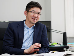
ProfessorAkira Ohtomo
Department of Applied Chemistry, Graduate School of Science and Engineering
Contributing to improvement of the quality of metal oxides
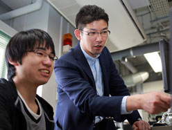
In a laboratory in a research building in the Ookayama South Area, in a room that is quiet except for the humming of experimental apparatus, a student is avidly staring into a monitor.
"I'm just observing the condition of the crystals using combinatorial chemistry [i] techniques. Crackling sounds are emitted from the laser that is employed for vaccum deposition of the solids."
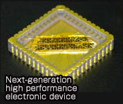
It has been nearly 20 years since Akira Ohtomo, head of the laboratory, became involved in research on the application of metal oxides to next-generation high performance electronic devices. Currently, mainstream materials used for semiconductor industry are non-oxides such as silicon (synthesized through the reduction of minerals such as metal oxides). Metal oxides are used as insulators to store static electricity in small parts of the devices or to prevent the flow of current. On the one hand, there were high hopes for metal oxides to be used in a variety of applications in electronics, as they exhibit a wide range of properties ranging from those of insulators to superconductors and even to magnets. Next-generation high performance electronic deviceHowever, because many impurities and defects form on the interfaces of different oxides, it has not been possible for them to be applied to next-generation high performance electronic devices, which require structures with few impurities over a large area. Given the current state of metal oxides, Ohtomo sought to improve the quality of their crystal structures. After many repeat trials and many new ideas of his own, Ohtomo's research results completely overturned current knowledge. He discovered the world's first metallic interface in the junction between insulators, which was thought to be impossible. For this series of research results, he was awarded the 9th Japan Academy Medal Prize in February 2013.
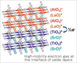
"Previously, the focus was on the structural properties of metal oxides, such as heat resistance and hardness, but in my case, I put them together in multilayers in a form of thin, pure crystals called 'thin films' and investigated the electrical properties at their interface. I discovered the phenomenon that while both layered crystalline structures were insulators, they were able to conduct electricity at their interface due to the presence of high-mobility electron gas. I also discovered the intriguing phenomenon that the electrons in one side that spill over to the other side due to the charge imbalance form two dimensional electrons at the interface, unlike the mechanism that was previously assumed".
Early interests sparked by EXPO '85, space shuttles and the superconductivity boom
There were several factors that led to Ohtomo getting involved in the world of semiconductor development. First, in tracing his roots, we are taken back to his final years in primary school. From March to September 1985 the International Science and Technology Exposition (Tsukuba Expo '85) was held in Tsukuba Science City. Ohtomo, who had just started junior high school at the time, visited the venue many times during that period, accompanied by his father.
"My father and I went there at least five times in total. Maybe because it was close to my house, but my father was also an electrical engineer, so he must have been interested in it too. His interest in electronics was so strong that on weekends, he used to tell me about the circuits and cathode ray tubes in televisions when I was only in primary school," Ohtomo reflects fondly.
The Expo showcased an array of pioneering technology, gathered from around the world. In addition, this was the time when the space shuttle program, which was launched in 1981, dominated everyday conversations. By the end of 1986, the high-temperature superconductivity boom was in full swing."I wanted to get involved in all kinds of new technology too," young Ohtomo's dreams grew bigger.
In his university entrance examination, Ohtomo had initially applied to the 4th Academic Group (the field of mechanical engineering) at Tokyo Institute of Technology. This decision was rooted in his admiration for the structure of space shuttles, and the desire to get involved in the construction of such complex systems himself. In the end however, he chose to enter the 2nd Academic Group (the field of materials), which had been his second choice, but was very much in line with his original dreams.
"The tiles covering all over the space shuttles are ceramics. I thought that if I research ceramics in the Department of Inorganic Materials, I might be able to get involved in space shuttle development in the future."
A decisive encounter occurred when he was a 3rd-year student. Ohtomo, who studied at the Ookayama Campus at the time, became interested in the superconductivity laboratory, which he learned about during Yacht Club camp. He visited the laboratory in Suzukakedai and immediately thought, "This is right for me!" and decided to enter this laboratory. At the time, Hideomi Koinuma, the authority in the field, was supervising there.
"I think it was when we went out for a drink, when Professor Koinuma suddenly said, 'Let's create electronics with metal oxides!' At the time, this was said to be impossible, so I was surprised. This is where my research started."
Drawing out the true potential of oxides and turning dreams into reality
Currently, there are three main research themes that Ohtomo is working on.
The first is "photocatalysis," a process in which chemical reactions are brought about through sunlight. In recent years photocatalysts have come into commercial use. One example is titanium dioxide on toilets which acts as an antibacterial. A property of titanium dioxide is its ability to break down harmful organic compounds when it is irradiated with ultraviolet light. In this way, a titanium dioxide coating effectively keeps toilets clean. Ohtomo continues to look ahead.
"To make a chemical reaction happen through the absorption of visible light, we actually need a non-transparent material. However, titanium dioxide is a colorless, clear material so there is only a small catalytic reaction with visible light. The search for a non-transparent material that works as a catalyst for photolysis of water with visible light is now attracting world attention."
As the non-transparent photocatalytic material, Ohtomo is focusing on "iron rust." If his persistence in improving the quality of metal oxide crystals pays off, they may be applied to the development of cars that can run on solar power alone, for example. The iron rust that we find around us can be used as a material to generate electricity. It is a dream-like scenario that makes us appreciate the potential of catalytic chemistry.
The second theme is the research and development of "power devices." Currently, there is a lot of focus on silicon carbide (SiC) as a next-generation power semiconductor with low electrical power loss. Ohtomo is conducting research in a collaborative team, which has discovered a material better than silicon carbide and is now investigating it.
The third theme revolves around "making electronic circuits on glass substrates," and is an extension of something called graphoepitaxy. Graphoepitaxy is a technique that was trendy in the 1980's and used in growing high quality semiconductors, whereby glass surfaces were made bumpy so that a layer of simple crystals called thin films would form. In this way many overlapping layers of simple crystal thin film semiconductors can be obtained. With this technique, it became possible to create large-area semiconductor substrates at a lower cost, which can then be used in applications such as substrates for solar cells and liquid crystal displays.
"By applying nanofabrication techniques to the glass surface, the synthesis progresses with the crystals arranged in arrays. In this way, you can create low-cost semiconductor substrates. The world would be quite different if you could make semiconductor substrates similar in quality to silicon wafers,[ii] but the size of a tatami mat (approximately 1.4m2), for 10,000 yen," Ohtomo's eyes lit up.
Finally, Ohtomo offers words of encouragement to students who have high hopes for the future.
"I often tell students, 'what matters most in research is allowing yourself to be inspired and having reserves of strength for the duration, because life is a long race.' You have to enjoy research. To do this, I want them to embrace new perspectives and make new discoveries. If you think of something yourself and realize it, you are left with excitement and a feeling of fulfillment. These experiences 'inspire.' Although, in reality, most of the time you fail. However, if you give up there, you can't experience the enjoyment of 'inspiration.' So I don't want them to forget their 'reserves of strength' and the prospect of a 'long race.'"
Ohtomo himself has not always travelled an easy road. When he belonged to Bell Laboratories in the U.S. as a postdoctoral member of the technical staff, he was troubled by the differences in research culture, and was distressed by an incident involving a colleague there who fabricated research papers. It was a mental blow. Perhaps it was his strong mind, which he cultivated during his time in the Yacht Club, that helped him to persevere through these difficult times.
"If you have a positive outlook and a resilient attitude in the face of defeat, where it is OK to fail now as long as you succeed later, the results will follow by themselves. I still believe this to be true."
[i] The technique where many groups of compounds are synthesized efficiently based on combinatorics, and using them according to different purposes.
[ii] An artificial crystal that is processed into sheet form, and is vital for integrated circuit technology. Without this, the IT society of today could not have been established.
Akira Ohtomo
Profile
- 2009Professor, Department of Applied Chemistry
Graduate School of Science and Engineering
- 2009Associate Professor, Institute for Materials Research
Tohoku University
- 2007Assistant Professor, Institute for Materials Research
Tohoku University
- 2002Research Associate, Institute for Materials Research
Tohoku University
- 2000Postdoctoral Member of Technical Staff, Materials Physics Department, Bell Laboratories, Lucent Technologies
- 2000Doctor of Engineering, Department of Innovative and
Engineered Materials, Interdisciplinary Graduate School of
Science and Engineering, Tokyo Institute of Technology
- 1972Born in Kanagawa
Major Awards
- 2013JSPS Prize, Japan Academy Medal Prize
- 2011Gottfried Wagener Prize
- 2007Sir Martin Wood Prize
The Special Topics component of the Tokyo Tech Website shines a spotlight on recent developments in research and education, achievements of its community members, and special events and news from the Institute.
Past features can be viewed in the Special Topics Gallery.